Flat panel display

a technology of flat panel display and display screen, which is applied in the direction of discharge tube luminescnet screen, identification means, instruments, etc., can solve the problems of reducing the emission region, affecting the quality of picture, and limiting the taper angle of contact or via hole, so as to prevent pinhole and short-circuit defects

Active Publication Date: 2005-06-02
SAMSUNG DISPLAY CO LTD
View PDF10 Cites 43 Cited by
  • Summary
  • Abstract
  • Description
  • Claims
  • Application Information

AI Technical Summary

Benefits of technology

[0020] The present invention provides an OLED capable of preventing pinhole and short-circuit defects in a contact hole and a via hole.
[0021] The present invention provides an OLED capable of improving a picture quality by reducing or preventing a pattern defect of an organic EL layer.
[0022] The present invention provides an OLED capable of reducing or preventing inflow of oxygen or moisture by densely forming a cathode electrode.
[0023] The present invention provides an OLED capable of reducing or preventing a dark spot from being occurred in an emission region of a pixel.
[0024] An exemplary embodiment of the present invention provides a flat panel display having an insulating substrate, a lower layer formed on the insulating substrate and having a first step and a first taper angle with respect to a surface of the substrate, and an upper layer formed on the insulating substrate and for reducing the taper angle of the lower layer, wherein the upper layer has a second taper angle smaller than the first taper angle of the lower layer.

Problems solved by technology

As a result, the emission region may decrease and the picture quality may deteriorate due to the occurrence of the dark spot.
However, there has been a limit in reducing the taper angle of the contact hole or via hole due to difficulties in design of a high resolution flat panel display.
However, in the high-resolution OLED, there has been a limit to reducing the taper angle of the passivation layer or the pixel defining layer due to difficulties in the design process.
When the taper angle is large, the organic emission layer and the cathode electrode easily deteriorate at the edge of the opening.
When the taper angle is small, there has been a limit to reducing the tape angle and thickness of the pixel defining layer due to problems of parasitic capacitance and a stepped portion caused by the wiring.

Method used


Image

  • Flat panel display
  • Flat panel display
  • Flat panel display

Examples


Embodiment Construction

[0053] The present invention will now be described more fully hereinafter with reference to the accompanying drawings, in which exemplary embodiments of the invention are shown. This invention may, however, be embodied in different forms and should not be construed as limited to the embodiments set forth herein. Rather, these embodiments are provided so that this disclosure will be thorough and complete, and will fully convey the scope of the invention to those skilled in the art. In the drawings, the thickness of layers and regions are exaggerated for clarity. Like numbers refer to like elements throughout the specification.

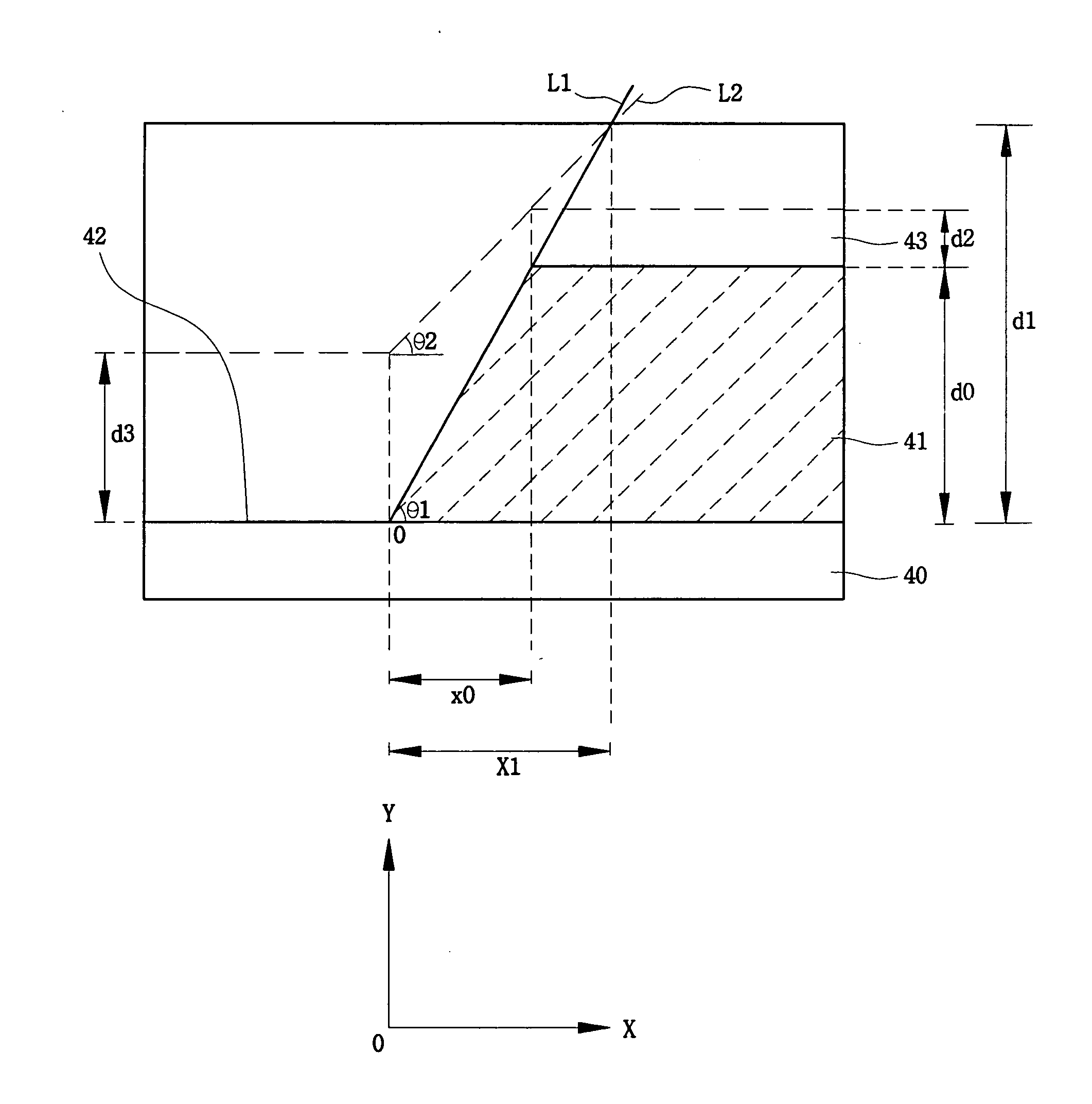
[0054]FIG. 4 illustrates a cross-sectional view of an OLED having a taper angle reduced by a taper reducing layer of the present invention. Referring to FIG. 4, an insulating substrate 40 has a lower layer 41 having an opening 42 for exposing a portion of the insulating substrate 40. The lower layer 41 has a predetermined taper angle with respect to an upper su...


PUM

PropertyMeasurementUnit
taper angleaaaaaaaaaa
taper anglesaaaaaaaaaa

Abstract

The present invention discloses an organic light emitting device for preventing element defects and improving picture quality by reducing a taper angle of a substrate surface. The flat panel display of the present invention comprises, an insulating substrate, a lower layer formed on the insulating substrate and having a first step and a first taper angle with respect to the substrate surface, and an upper layer formed on the insulating substrate and for reducing the taper angle of the lower layer. The upper layer has a second taper angle smaller than the first taper angle of the lower layer. The upper layer is a conductive layer that may be applied by a wet coating method, has a charge transporting capability, and is selected from at least one of a small-molecule organic layer including a carbazole-based, arylamine-based, hydrazone-based, stilbene-based, oxadiazole-based, starburst-based derivatives, and a polymer organic layer including PEDOT, PANI, carbazole-based, arylamine-based, perylene-based, pyrrole-based, oxadiazole-based derivatives.

Description

CROSS-REFERENCE TO RELATED APPLICATION [0001] This application claims the benefit of Korea Patent Application No. 2003-84746, filed on Nov. 26, 2003, the disclosure of which is incorporated herein by reference in its entirety. BACKGROUND OF THE INVENTION [0002] 1. Field of the Invention [0003] The present invention relates to a flat panel display and, more particularly, to an active matrix organic light emitting device capable of avoiding a defective element and improving picture quality by reducing a taper angle of a substrate surface. [0004] 2. Background of the Invention [0005] In general, pixels in an active matrix organic light emitting device (AMOLED) are arranged on the substrate in a matrix form. Each pixel includes an electroluminescence (EL) element, where an anode electrode, an organic film layer and a cathode electrode are stacked, and a thin film transistor (TFT) as an active element connected to the EL element and for driving the EL element. [0006]FIG. 1A shows a cross...

Claims


Application Information

Patent Timeline
Patent Type & Authority Applications(United States)
IPC IPC(8): H05B33/22C09K11/06G09F9/30H01L27/00H01L27/32H01L51/50H01L51/52H05B33/00H05B33/02H05B33/12H05B33/14H05B33/20
CPCH01L27/3244H01L27/3246H01L27/3248Y10T428/24479H01L51/52H01L51/5203Y10T428/24521H01L51/5048H10K59/122H10K59/123H10K59/12H10K50/14H10K50/80H10K59/805H05B33/22H10K50/805
Inventor KIM, MU-HYUNCHIN, BYUNG-DOOSONG, MYUNG-WONLEE, SEONG-TAEK
Owner SAMSUNG DISPLAY CO LTD
Why Eureka
Try Eureka