Substrate for mounting semiconductor chip, mounting structure of semiconductor chip, and mounting method of semiconductor chip

a technology for mounting semiconductor chips and semiconductor chips, which is applied in the direction of printed circuit manufacturing, printed circuit electric connection formation, printed circuit aspects, etc., can solve the problems of difficult application into such mobile computers to be placed under severe operation environment, broken connection parts, etc., to achieve strong and stable connection, improve stress relief capability of wiring portions, and improve the effect of connection reliability

Active Publication Date: 2005-06-02
DENSO CORP
View PDF4 Cites 11 Cited by
  • Summary
  • Abstract
  • Description
  • Claims
  • Application Information

AI Technical Summary

Benefits of technology

[0029] The mounting structure of semiconductor chip according to a twenty-third aspect is characterized in that the semiconductor chip where a stud bump is formed to an electrode is bonded, in the face down manner, to the substrate for mounting semiconductor chip according to twenty-first aspect from the surface opposed to the surface where a part of the wire is projected to the aperture of the through-hole under the condition that the electrode and through-hole of the semiconductor chip are matched in the position, the wire projected to the aperture is bonded to the stud bump of the semiconductor chip, and thereby the wire and electrode of semiconductor chip are electrically connected. According to this mounting structure of semiconductor chip, since the wire of the connecting portion to the semiconductor chip is not fixed to the insulation base material, the stress alleviating capability of wiring portion can be improved and thereby higher connection reliability can be attained. Moreover, the wire projected to the aperture of the through-hole sticks to stud bump due to the plastic deformation of stud bump. Accordingly, more strong and stable connection can be obtained.
[0030] The mounting structure of the semiconductor chip according to a twenty-fourth aspect is characterized in that the semiconductor chip where a plated bump is formed to an electrode is bonded, in the face down manner, to the substrate for mounting a semiconductor chip according to a twenty-first aspect from the surface opposed to the surface where a part of wire is projected to the aperture of through-hole under the condition that the electrode and through-hole of the semiconductor chip are matched in the position, the wire projected to the aperture is bonded to the plated bump of semiconductor chip, and the wire and electrode of semiconductor chip are electrically connected. According to this mounting structure of semiconductor chip, since the wire of the connecting portion to the semiconductor chip is not fixed to the insulation base material, the stress alleviating capability of the wiring portion can be improved and thereby higher connection reliability can be attained. Moreover, since the plated bump can be formed simultaneously under the wafer condition, manufacturing cost can be lowered in comparison with that of the stud bump.
[0031] The mounting method of semiconductor chip according to a twenty-fifth aspect is characterized by comprising the first process for mounting, in the face down manner, through a bonding agent, the semiconductor chip to the surface opposing to the surface where a part of the wire is projected to the aperture of through-hole in the substrate for mounting a semiconductor chip according to the twenty-first aspect under the condition that the electrode and through-hole of the semiconductor chip are matched in the position, and the second process for bonding the wire projected to the aperture to the electrode of semiconductor chip using the bonding tool from the surface where a part of wire is projected to the aperture of through-hole in the substrate for mounting the semiconductor chip. According to this mounting method of semiconductor chip, since the wire of the connecting portion to the semiconductor chip is not fixed to the insulation base material, the stress alleviating capability of wiring portion can be improved and higher connection reliability can also be attained.
[0032] In the invention according to a twenty-sixth aspect, the insulation base material is formed of thermosetting resin base material in the substrate for mounting semiconductor chip according to the fourteenth or twenty-first aspects. Moreover, in the twenty-seventh aspect, the substrate for mounting semiconductor chip accordi

Problems solved by technology

Therefore, stress generated due to difference in the line expansion coefficients of the semiconductor chip 110 and substrates 100 and 120 is concentrated to the bonding area of the bump 111 and substrates 100 and 120, resulting in t

Method used


Image

  • Substrate for mounting semiconductor chip, mounting structure of semiconductor chip, and mounting method of semiconductor chip
  • Substrate for mounting semiconductor chip, mounting structure of semiconductor chip, and mounting method of semiconductor chip
  • Substrate for mounting semiconductor chip, mounting structure of semiconductor chip, and mounting method of semiconductor chip

Examples


first embodiment

[0065] The first embodiment embodying the present invention will be described below in accordance with the accompanying drawings.

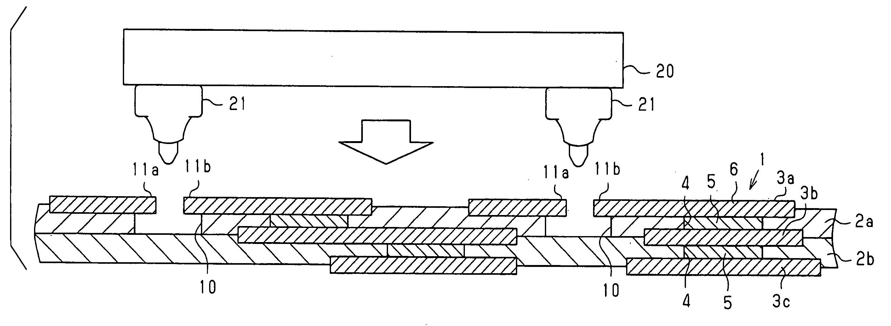
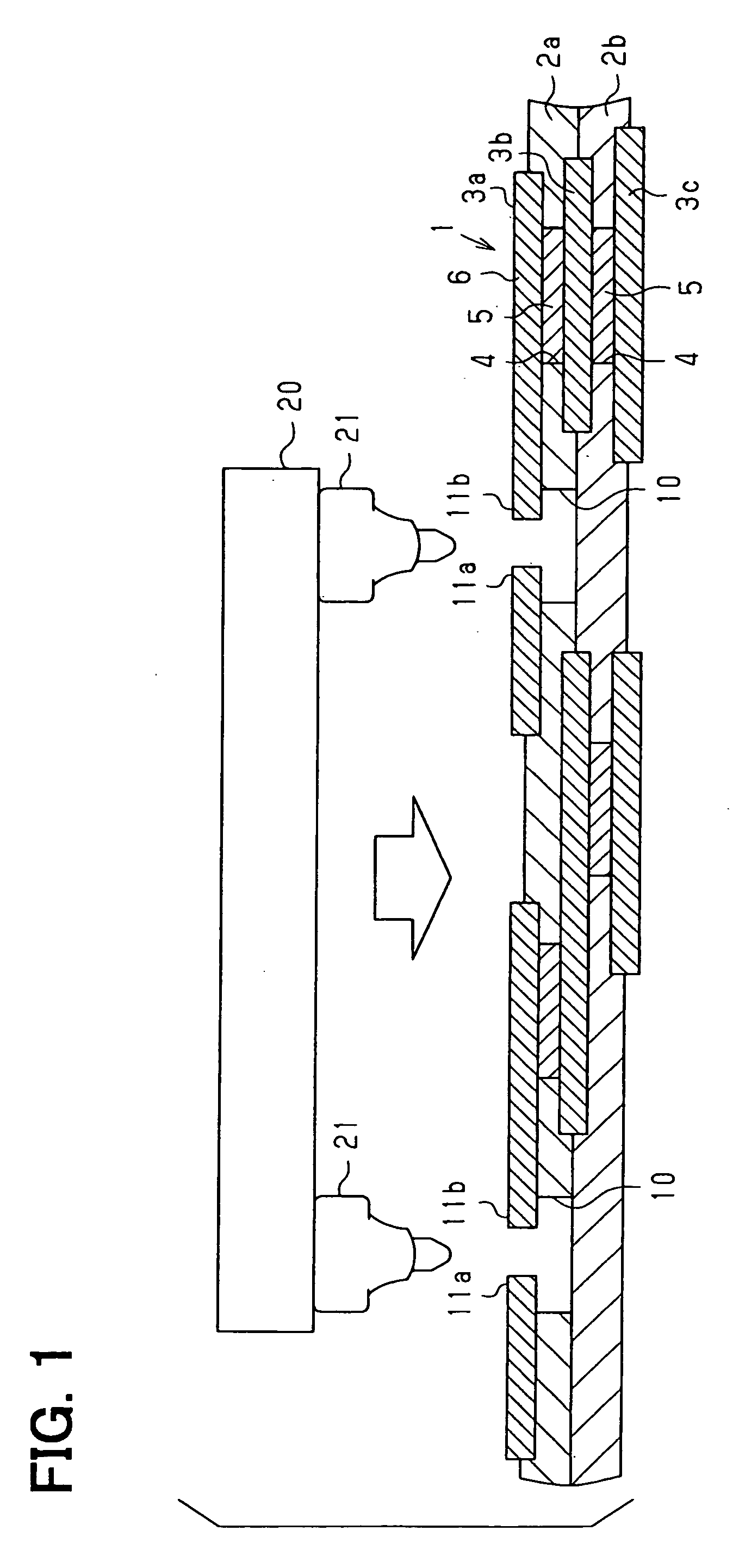
[0066] In FIG. 1, a substrate 1 for mounting a semiconductor chip and a semiconductor chip 20 before the mounting in this first embodiment are illustrated. A mobile computer (electronic control apparatus) is constructed by the substrate 1 for mounting semiconductor chip, the semiconductor chip 20, and the like. The semiconductor chip 20 is provided with bumps (projected electrodes) 21.

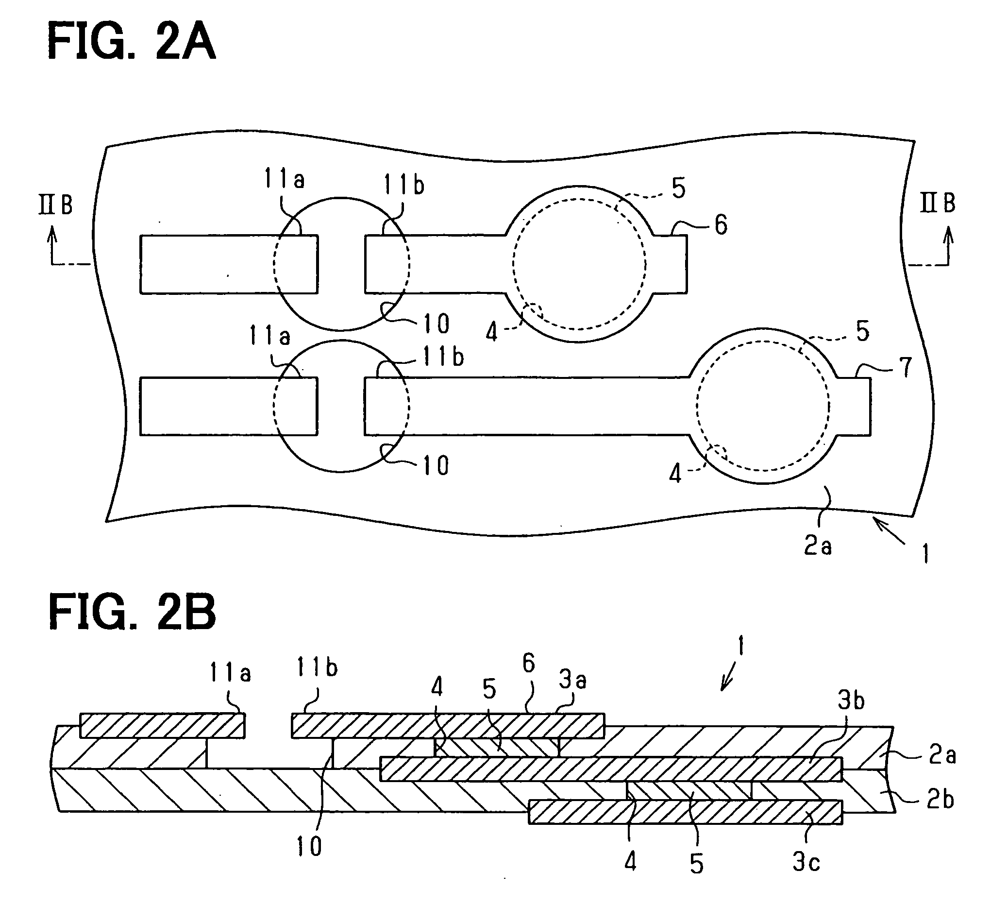
[0067]FIGS. 2A and 2B are partially enlarged views of the substrate 1 for mounting the semiconductor chip. FIG. 2A is a plan view of the substrate 1, while FIG. 2B is a cross-sectional view along the line IIB-IIB of FIG. 2A. In these FIGS. 2A and 2B, the substrate 1 for mounting the semiconductor chip is formed by alternately stacking the insulation layers (base materials) 2a, 2b, etc. and wiring layers 3a, 3b, 3c, etc. to the insulation layers (base materials) 2a, 2b, etc....

second embodiment

[0080] Next, the second embodiment will be described with reference to the accompanying drawings.

[0081]FIGS. 9A and 9B illustrate the substrate 50 for mounting the semiconductor chip 20 and the semiconductor chip 20 itself in this embodiment. FIG. 9A illustrates the condition before the mounting and FIG. 9B illustrates the condition after the mounting.

[0082]FIGS. 10A and 10B are partially enlarged diagrams of the substrate 50 for mounting semiconductor chip, in which FIG. 10A is a plan view of the substrate 50 and FIG. 10B is a cross-sectional view along the line XB-XB in FIG. 10A. In FIGS. 10A and 10B, the substrate 50 for mounting the semiconductor chip is formed by alternately stacking the insulation layers (base materials) 51a, 51b, etc. and wiring layers 52a, 52b, etc. The insulation layers (base materials) 51a, 51b, etc. are also provided with via-holes 54 for interlayer continuity to electrically connect the wiring of each layer. The wire of each layer is electrically conne...

third embodiment

[0108] Next, the third embodiment will be described with reference to the accompanying drawings.

[0109]FIGS. 17A and 17B are vertical cross-sectional views before and after the mounting of the semiconductor chip in this third embodiment. FIG. 18A is an enlarged plan view of the substrate 80 for mounting the semiconductor chip in this embodiment, while FIG. 18B is a vertical cross-sectional view along the line XVIIIB-XVIIIB in FIG. 18A.

[0110] In FIGS. 18A and 18B, the substrate 80 for mounting the semiconductor chip includes the wire 82 patterned over the surface of the insulation base material sheet 81. As the insulation base material 81, the glass and epoxy base materials can be used. Moreover, the wire 82 is constructed by sequentially forming the nickel film and gold plated film over the patterned copper foil. The semiconductor chip 20 is flip chip mounted on this substrate 80 for mounting semiconductor chip.

[0111] Moreover, the through-hole 83 is formed through the insulation ...


PUM


Abstract

A substrate for mounting a semiconductor chip is formed as a multilayer substrate by alternately laminating insulation layers and wiring layers. Wires of the wiring layers are electrically connected through a via-hole for interlayer continuity. A through-hole provided through the insulation layer of the outermost surface layer is formed. A bump is inserted in the through-hole to a bump allocating position of the semiconductor chip to be mounted in the insulation layer of the outermost surface layer. A portion of the wire in the wiring layer of the outermost surface layer is projected to the internal side of through-hole at the aperture of the through-hole.

Description

CROSS REFERENCE TO RELATED APPLICATIONS [0001] This application is based upon, claims the benefit of priority of, and incorporates by reference the contents of Japanese Patent Application No. 2003-397794 filed on Nov. 27, 2003 and Japanese Patent Application No. 2004-210626 filed on Jul. 16, 2004. FIELD OF THE INVENTION [0002] The present invention relates generally to a substrate for mounting a semiconductor chip, a mounting structure of semiconductor chip, and a mounting method of semiconductor chip. BACKGROUND OF THE INVENTION [0003] Wire bonding and flip chip mounting have been proposed as methods for mounting a semiconductor chip. FIG. 28A illustrates a cross-sectional view of a flip chip mounted to a laminated substrate 100. In the flip chip mounting, a semiconductor chip 110 is mounted face down on the substrate 100 and connected to the substrate 100 through bumps 111. When high density mounting is required, a bonding pad is unnecessary for the periphery of semiconductor chip...

Claims


Application Information

Patent Timeline
IPC IPC(8): H01L23/12H01L21/60H01L23/498H05K3/32H05K3/34H05K3/40
CPCH01L23/49816H01L23/49822H01L23/49827H01L23/49838H01L24/16H01L24/48H01L24/50H01L24/78H01L24/83H01L24/85H01L24/90H01L2224/05599H01L2224/1134H01L2224/13099H01L2224/13144H01L2224/16225H01L2224/16237H01L2224/45144H01L2224/4824H01L2224/48245H01L2224/48465H01L2224/48599H01L2224/73204H01L2224/73215H01L2224/78H01L2224/83192H01L2224/838H01L2224/85399H01L2224/92147H01L2924/01004H01L2924/01005H01L2924/01006H01L2924/01014H01L2924/01028H01L2924/01029H01L2924/01047H01L2924/01078H01L2924/01079H05K3/326H05K3/3436H05K3/4092H05K2201/0397H05K2201/1059H05K2201/10674H01L24/45H01L2224/2919H01L2924/01033H01L2924/01065H01L2924/0665H01L2224/81899H01L2224/48247H01L2224/81191H01L2924/00014H01L2224/1624H01L2224/32225H01L2924/10253H01L2224/0401H01L2924/00H01L2924/351H01L2924/12042H01L2224/85205H01L24/81H01L24/86
Inventor KASHIWAZAKI, ATSUSHI
Owner DENSO CORP
Why Eureka
Try Eureka