Light emitting device

a technology of light-emitting devices and light-emitting components, which is applied in the direction of semiconductor devices, basic electric elements, electrical equipment, etc., can solve the problems of increasing the manufacturing cost, limiting the light output, and heat generation, and achieves simple configuration, high light emission efficiency, and easy fabrication

Active Publication Date: 2005-06-09
SUMITOMO ELECTRIC IND LTD
View PDF16 Cites 198 Cited by
  • Summary
  • Abstract
  • Description
  • Claims
  • Application Information

AI Technical Summary

Benefits of technology

[0018] It is an object of the present invention to provide light emitting devices which have a simple configuration thereby making it easy to fabricate, can provide a high light emission efficiency for a long time period, and can be easily miniaturized.

Problems solved by technology

On the other hand, the aforementioned GaN-type LED using a sapphire substrate illustrated in FIG. 51 has a complicated construction, which unavoidably increases the fabrication cost.
However, the construction illustrated in FIG. 51 restricts the areas, thus restricting the light output.
Further, there is a large resistance to currents flowing in the direction parallel to n-type GaN layer 102, which may cause heat generation and, therefore, increases in the power consumption.
Particularly, in the case where the thickness of the n-type GaN layer is reduced in order to shorten the film formation processes, the yield of exposure of the n-type GaN film is degraded, in addition to the aforementioned heat generation and power consumption increases.
Further, it can be said for light emitting devices in general that the heat radiating area is restricted and also the heat resistance (the temperature rise due to unit energy introduced per unit area) is large, and therefore the injected current per single light emitting device can not be made large.
Further, since the aforementioned GaN-type LED using a sapphire substrate restricts the heat radiating area, it unavoidably becomes necessary to utilize a configuration including intricate comb-shaped p-electrode and n-electrode for increasing the contact area therebetween.
It is not easy to manufacture these comb-shaped electrodes, thereby certainly increasing the manufacture cost.
When an attempt is made to generate high outputs, the aforementioned heat conditions introduce restrictions thereto, and therefore it is unavoidably required to use complicated electrodes in order to alleviate them as much as possible.
Further, there is a problem as follows.
This reduces the light emitting efficiency at the main surface of the sapphire substrate.
This problem of the light emitting efficiency is important.
However, there are still other problems.
This will damage resin which is placed at the side portions of the GaN layer and thus irradiated with the light.
This will induce a problem of shortening the life of the light emitting device.
Further, with a GaN-type LED having a construction of (an n-electrode on the back surface of a SiC substrate / SiC substrate / n-type GaN layer / quantum well laminated-layer construction (light emitting layer) / p-type GaN layer / p-electrode) which emits light from the p-layer side, light can not be efficiently emitted to the outside because of the high light absorption at the p-electrode.
Therefore, light emission can not be activated through the entire quantum well construction, thereby decreasing the light emission output.
Furthermore, the electric resistance will be increased, which will induce problems of heat generation and power supply capacity.
Also, if an attempt is made to increase the thickness of the p-type GaN layer in order to uniformly flow currents through the entire p-type GaN layer, this will restrict the output since this p-type GaN layer will absorb a large amount of light.

Method used


Image

  • Light emitting device
  • Light emitting device
  • Light emitting device

Examples


first embodiment

[0092] In the first embodiment, side-view type LEDs were fabricated using light emitting devices p-top (n-down) mounted on GaN substrates and including an n-electrode formed on the back side of the GaN substrate according to the present embodiment. Further, side-view type LEDs were fabricated using conventional light emitting devices. Then, comparison was made therebetween in terms of the size, light output and luminance.

(Invention Sample A)

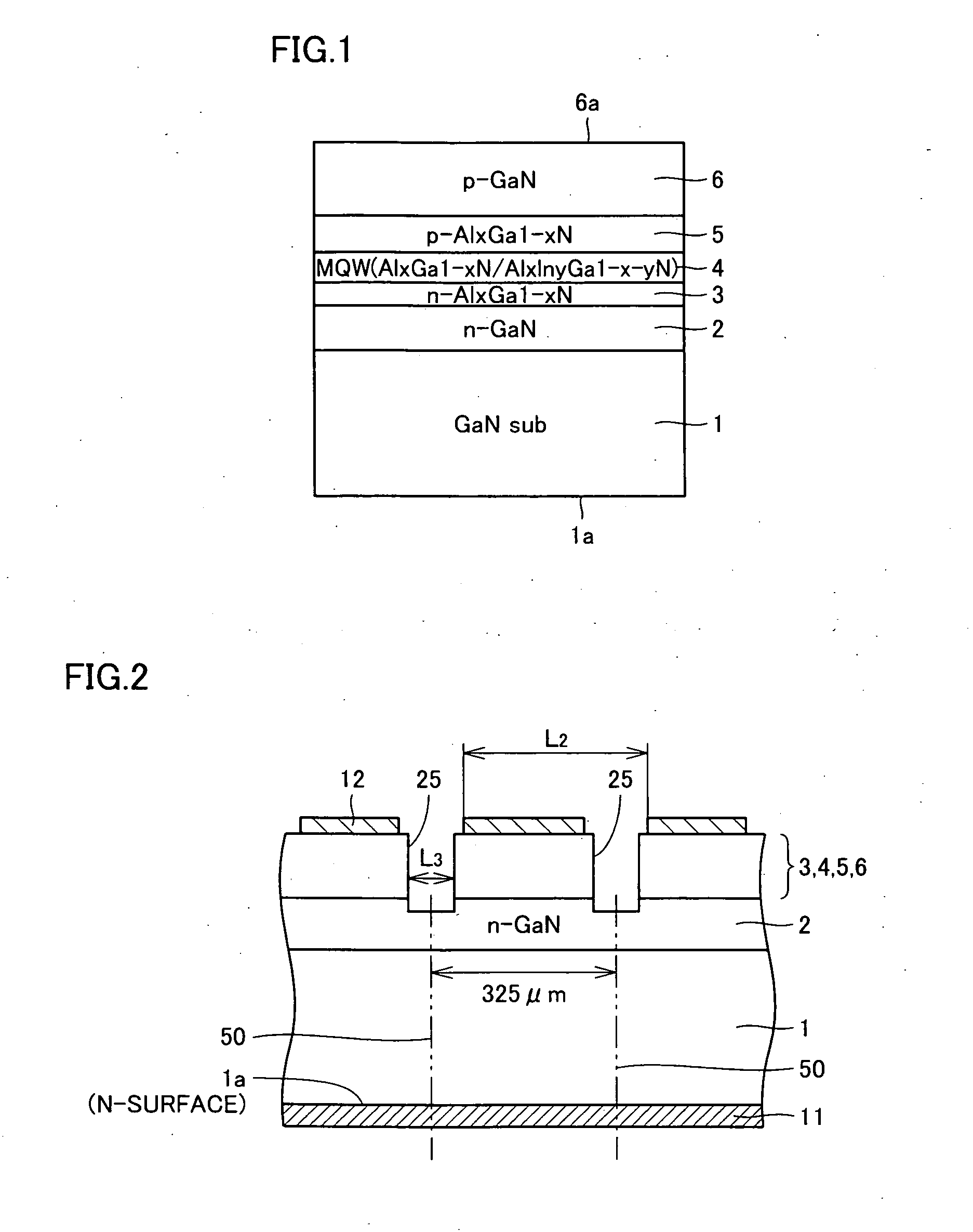
[0093] Referring to FIG. 1, there is formed a laminate construction of an n-type GaN layer 2 / an n-type AlxGa1−xN layer 3 / a multi quantum well layer (active layer) 4 consisting of (AlxGa1−xN / AlxInyGa1−x−yN)m / an p-type AlxGa1−1N layer 5 / an p-type GaN layer 6 which have been formed on the surface (first main surface) of a GaN substrate 1 by epitaxial film formation in order from the bottom side. The multi quantum well layer may be formed from (GaxN / InxGa1−xN)m. The number of laminated sets is usually 3, but may be more. The light emitting surface...

second embodiment

[0133] The second embodiment of the present invention was characterized in that an invention sample C, an invention sample D and a comparison sample E were p-down-mounted and the back surface of the n-type layers or the n-type semiconductor substrate was used as a light emitting surface. Invention sample D had a dislocation density of 1E9 / cm2, which was out of the range of dislocation density of light emitting devices according to the present invention employing a nitride semiconductor substrate having a reduced dislocation density. However, invention sample D was included in other types of light emitting devices according to the present invention. In the present embodiment, a sapphire substrate was employed to form comparison sample E and an attempt was made to provide an n-electrode and a p-electrode on the laminated-layers side of the sapphire substrate and down-mount these two electrode. However, an n-electrode having the same size as that of invention samples C, D could not be ...

third embodiment

[0153] In the third embodiment, performance such as the light output was examined for an invention sample F which was a light emitting device provided by applying a non-mirror-surface treatment to the aforementioned invention sample C and for a light emitting device provided with a reflective layer between the light emitting layer and the mounting portion (lead frame, etc.).

(Invention Sample F)

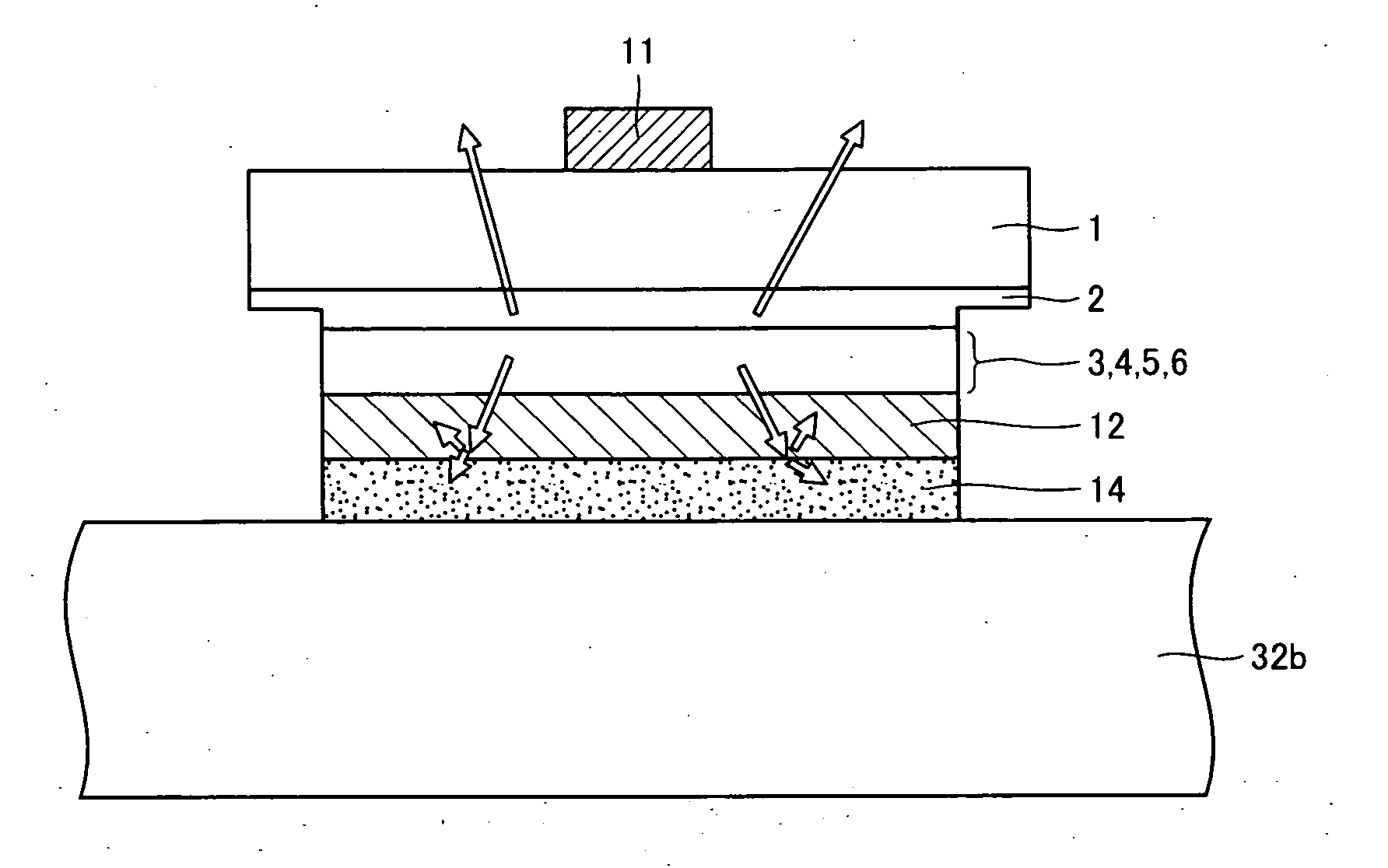
[0154] Referring to FIG. 20, a non-mirror-surface treatment has been applied to the back surface of the GaN substrate forming a light emitting surface and the side surfaces of the GaN surface and the side surfaces of the laminated-layer construction. Namely, the N-surface of the GaN substrate and the end surfaces of the device were made to be non-mirror surfaces. For comparison, FIG. 21 illustrates an image of light being emitted from light emitting device 10 having mirror surfaces.

[0155] As the method for forming non-mirror surfaces, there are methods using dry etching such as RIE or wet ...


PUM


Abstract

A light emitting device includes a nitride semiconductor substrate with a resistivity of 0.5 Ω·cm or less, an n-type nitride semiconductor layer and a p-type nitride semiconductor layer placed more distantly from the nitride semiconductor substrate than the n-type nitride semiconductor layer at a first main surface side of the nitride semiconductor substrate, and a light emitting layer placed between the n-type nitride semiconductor layer and the p-type nitride semiconductor layer, wherein one of the nitride semiconductor substrate and the p-type nitride semiconductor layer is mounted at the top side which emits light and the other is placed at the down side, and a single electrode is placed at the top side. Therefore, there is provided a light emitting device which has a simple configuration thereby making it easy to fabricate, can provide a high light emission efficiency for a long time period, and can be easily miniaturized.

Description

BACKGROUND OF THE INVENTION [0001] 1. Field of the Invention [0002] The invention relates to light emitting devices and more particularly to light emitting devices formed from nitride semiconductors. Hereinafter, “a light emitting device” refers to “a light emitting element” or “a mounted light emitting element construction equipped with a light emitting element”, unless otherwise mentioned. [0003] 2. Description of the Background Art [0004] White light emitting diodes (LED) have been widely utilized for illumination for the display devices of portable information terminals, etc., including portable phones. In the case of using LEDs as the light source of the display device of a portable information terminal, it is required to enhance the light emission performance. Therefore, there has been suggested a configuration for preventing light emitting unevenness in fabricating a side-view type LED equipped with a GaN-type light emitting device which has been assembled using a sapphire su...

Claims


Application Information

Patent Timeline
Patent Type & Authority Applications(United States)
IPC IPC(8): H01L33/12H01L33/32H01L33/42H01L33/50H01L33/56H01L33/60H01L33/62
CPCH01L33/02H01L2924/12041H01L33/22H01L33/32H01L33/38H01L33/58H01L2224/48247H01L2224/48465H01L2924/01004H01L2924/01012H01L2924/01013H01L2924/01029H01L2924/01046H01L2924/01078H01L2924/01079H01L2924/19041H01L33/0075H01L2924/01019H01L2224/73265H01L2224/48091H01L2224/32245H01L2224/45144H01L33/20H01L2924/00H01L2924/00014
Inventor NAGAI, YOUICHIKIYAMA, MAKOTONAKAMURA, TAKAOSAKURADA, TAKASHIAKITA, KATSUSHIUEMATSU, KOJIIKEDA, AYAKOKATAYAMA, KOJIYOSHIMOTO, SUSUMU
Owner SUMITOMO ELECTRIC IND LTD
Why Eureka
Try Eureka