

Method for handling semiconductor layers in such a way as to thin same
a technology of semiconductor layers and layers, applied in the direction of microstructural technology, electric devices, solid-state devices, etc., can solve the problems of reducing the thickness of wafers, affecting the thickness of structures, and affecting the effect of thickness
- Summary
- Abstract
- Description
- Claims
- Application Information
AI Technical Summary
Benefits of technology
Problems solved by technology
Method used
Image

Examples
Embodiment Construction
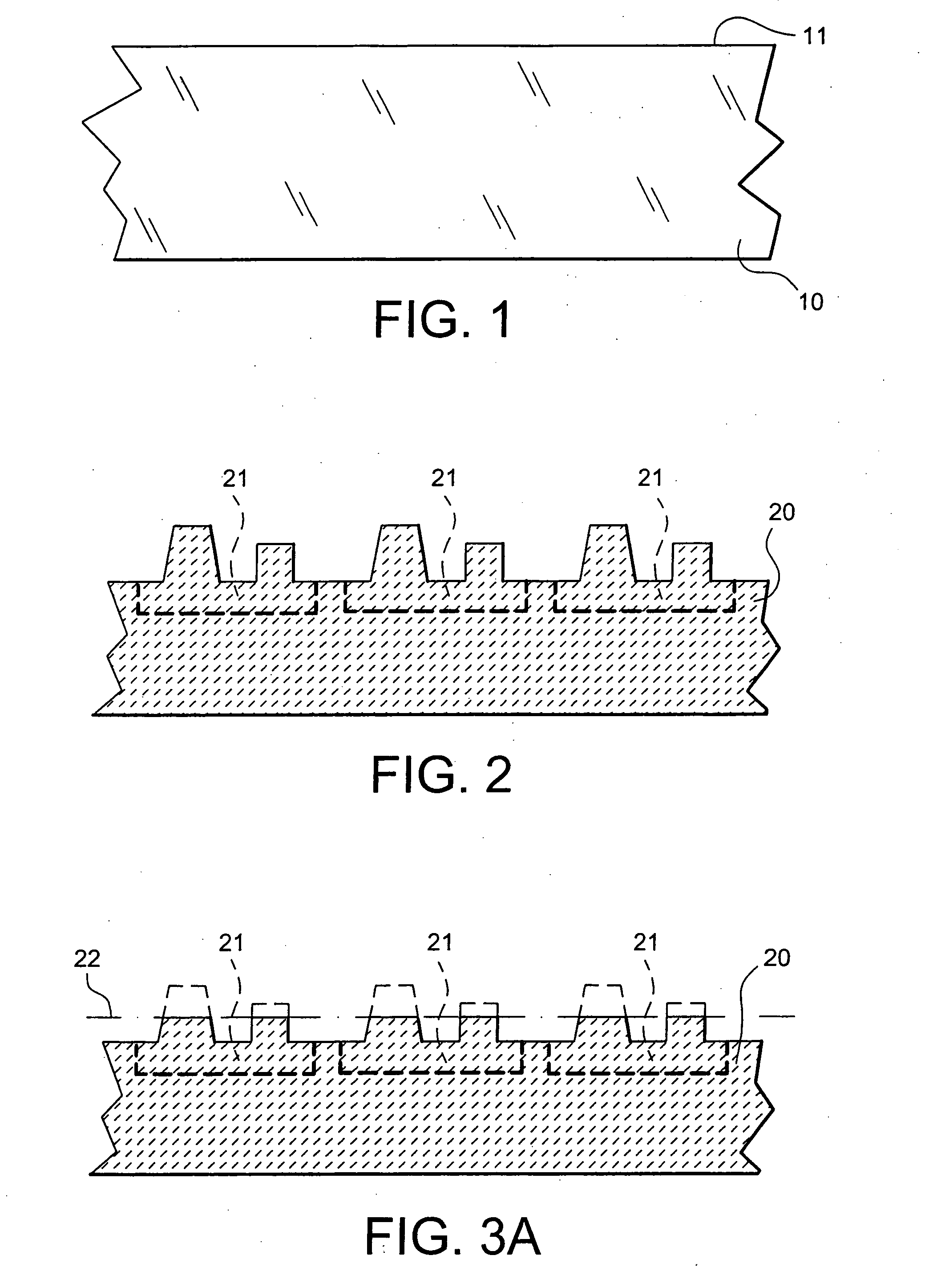
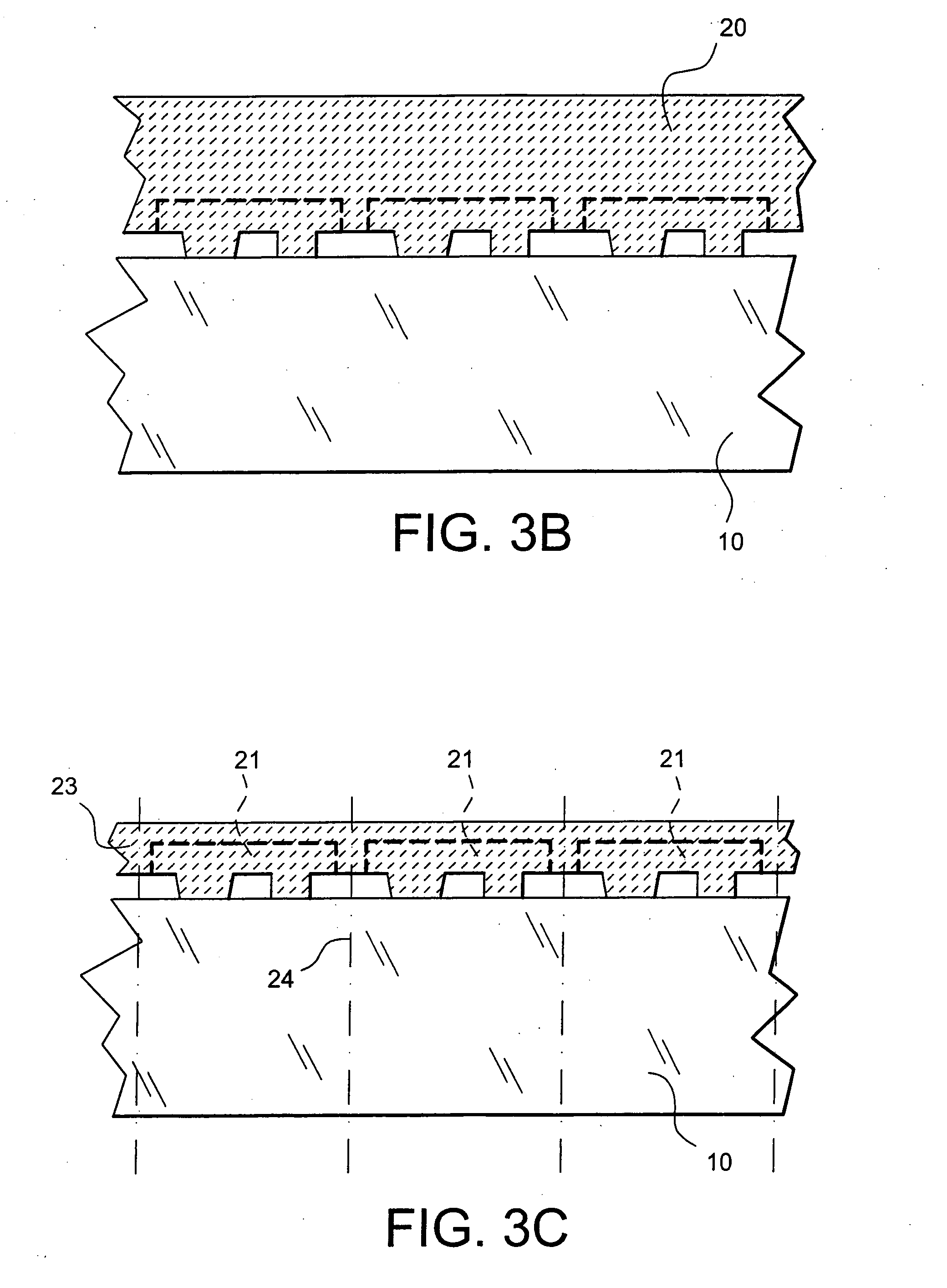
[0046]FIG. 1 is a cross-sectional view of a support handle 10, for example composed of a silicon or glass wafer. Glass has the advantage of being transparent, so that objects deposited on the back face can be inspected visually. The support handle 10 has a face 11 prepared to act as a bonding face.
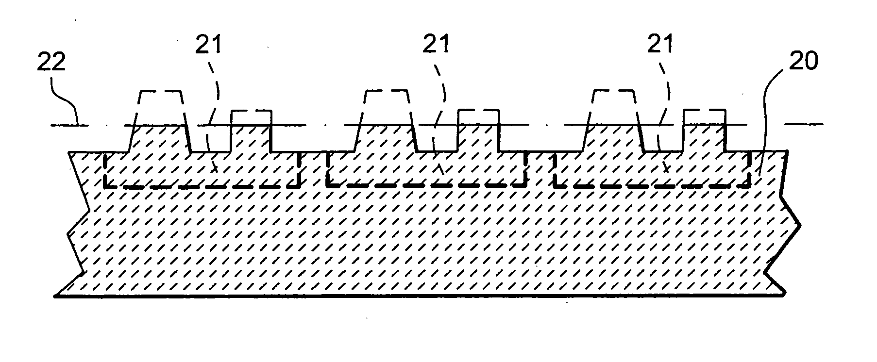
[0047]FIG. 2 is a cross-sectional view of a wafer 20 made of a semiconducting material, for example silicon. One of its main faces has been treated to make electronic components. FIG. 2 is a partial view showing three complete or incomplete components 21. Due to the presence of these components, that the treated plane face has a large relief with several areas of different heights and different roughnesses. When the wafer comprises complete components, part of this relief corresponds to the presence of openings used to connect to electrical contacts.
[0048] In general, the chemical nature of the wafers to be bonded by molecular bonding, chemical cleaning before bonding and the bonding con...
PUM
 Abstract
Description
Claims
Application Information