Novel multi-gate formation procedure for gate oxide quality improvement

Inactive Publication Date: 2005-06-09
TAIWAN SEMICON MFG CO LTD
View PDF11 Cites 11 Cited by
  • Summary
  • Abstract
  • Description
  • Claims
  • Application Information

AI Technical Summary

Benefits of technology

[0007] It is another object of this invention to use a photoresist shape to protect a first gate insulator layer located on first portions of a semiconductor substrate, during the wet etch removal of the same first insulator layer from second portions of a semiconductor substrate, wherein the second portions of the semiconductor subst

Problems solved by technology

However the process sequences used to form dual gate insulator layers can result in unwanted device leakage phenomena.
However the procedure used to subsequently remove the photoresist mask from the underlying firs

Method used


Image

  • Novel multi-gate formation procedure for gate oxide quality improvement
  • Novel multi-gate formation procedure for gate oxide quality improvement
  • Novel multi-gate formation procedure for gate oxide quality improvement

Examples


Embodiment Construction

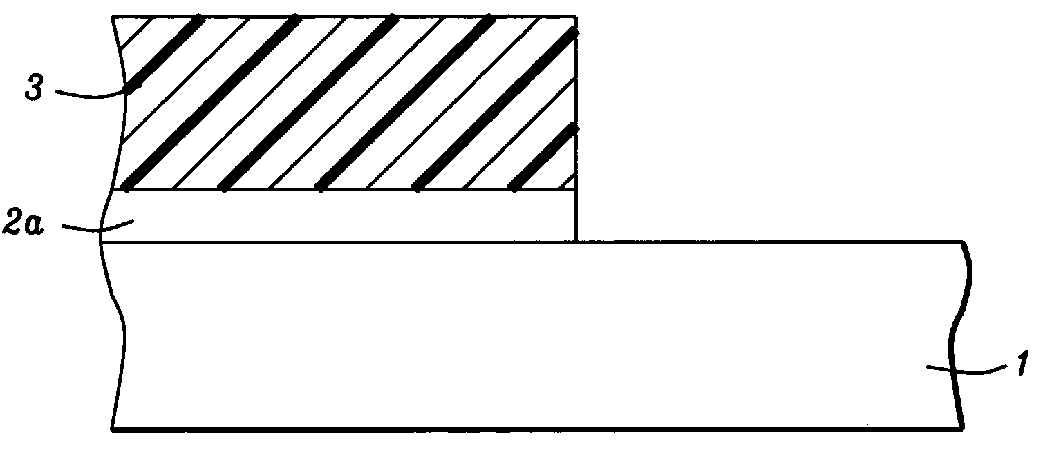
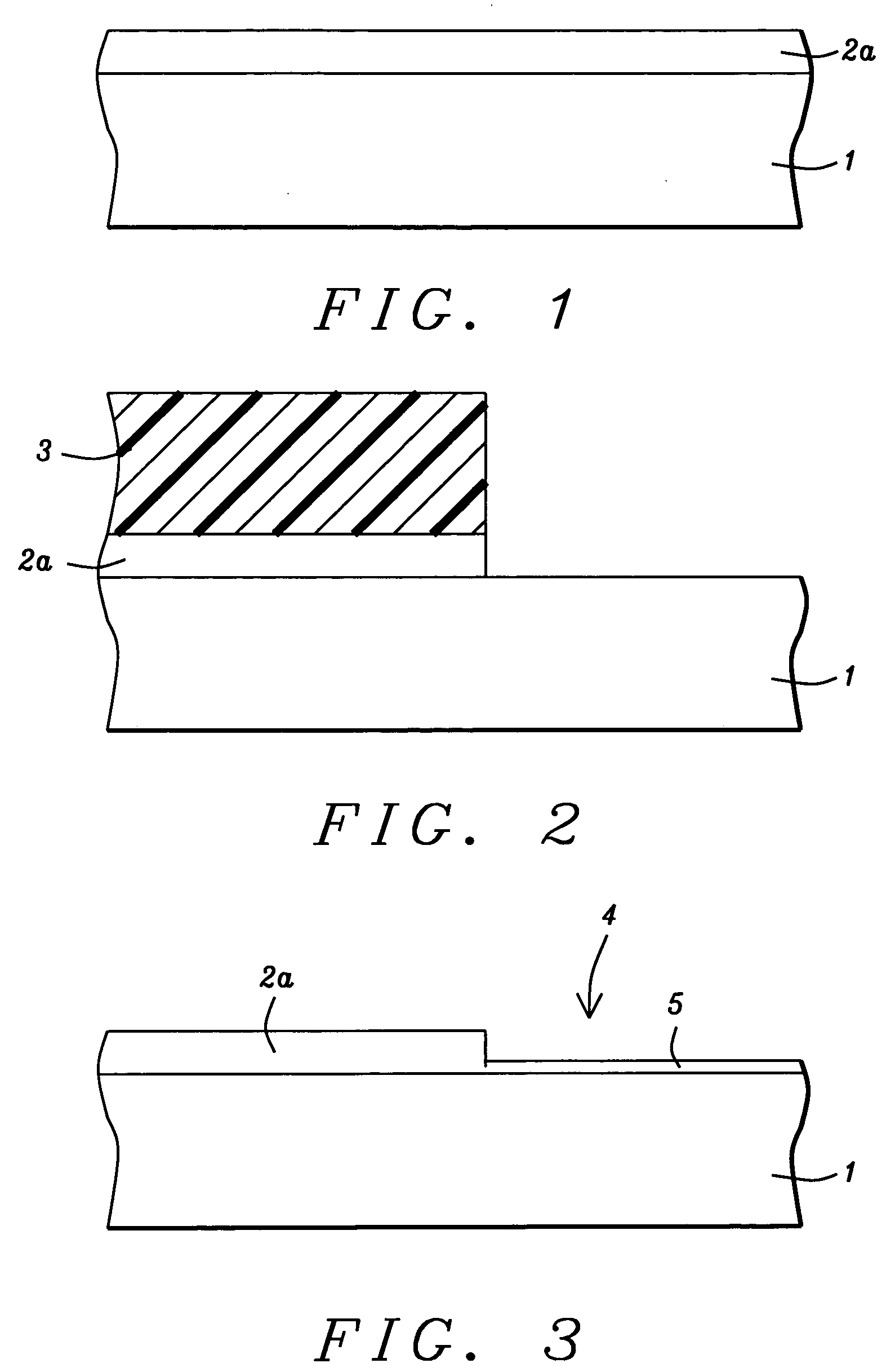
[0012] The method of fabricating multiple gate insulator layers on the same semiconductor substrate wherein the bare surface of a second section of semiconductor substrate, to be used to accommodate a subsequent second gate insulator layer, is protected from a procedure used to remove a photoresist masking shape from a first gate insulator layer overlying a first section of the semiconductor substrate, will now be described in detail. Semiconductor substrate 1, comprised of single crystalline silicon featuring a crystallographic orientation, is used. Gate insulator layer 2a, shown schematically in FIG. 1, comprised of silicon dioxide, is thermally grown in an oxygen-steam ambient at a thickness between about 10 to 200 Angstroms. Photoresist shape 3, is formed on a portion of gate insulator layer 2a, allowing the exposed portion of gate insulator layer 2a, to be removed via wet etch procedures featuring the use of either a buffered hydrofluoric (BHF) acid solution, or a dilute hydro...


PUM


Abstract

A process for forming a semiconductor device with multiple gate insulator thicknesses, wherein exposed surfaces of a semiconductor substrate are protected during a photoresist stripping procedure, has been developed. After growth of an insulator layer on the entire surface of a semiconductor substrate portions of the insulator layer not covered by a photoresist masking shape are selectively removed. A two step photoresist removal procedure is then employed initiating with an ozone water cycle which partially removes the photoresist shape while forming a thin silicon oxide layer on the portions of bare semiconductor surface. A acid-hydrogen peroxide mixture (SPM), is then used to complete the photoresist removal procedure including removal of photoresist residues, with the thin silicon oxide layer formed during the ozone water cycle protecting the previously bare underlying semiconductor surface. An oxidation procedure is then performed allowing a first gate insulator layer to be formed incorporating the original insulator layer, and allowing a thinner, second gate insulator layer to be obtained, incorporating the thin silicon oxide layer.

Description

BACKGROUND OF THE INVENTION [0001] (1) Field of the Invention [0002] The present invention relates to methods used to fabricate semiconductor devices and more specifically to a method used to form multi-gate oxide layers on a semiconductor substrate. [0003] (2) Description of Prior Art [0004] Specific semiconductor devices designed to provide dual voltage applications, particularly for the deep sub-micron technology, are achieved using two different gate insulator layer thicknesses, sometimes referred to as a dual gate oxide technology. However the process sequences used to form dual gate insulator layers can result in unwanted device leakage phenomena. For example a process used to form two different gate insulator layers entails growth of a first insulator layer on the entire surface of a semiconductor substrate, followed by removal of the first insulator layer from a second portion of the semiconductor substrate, so that the second portion of semiconductor substrate can be availa...

Claims


Application Information

Patent Timeline
IPC IPC(8): B32B3/02H01L21/283H01L21/302H01L21/461H01L21/8234
CPCH01L21/823462
Inventor CHIU, YI SONGCHENG, CHUNG LONGTSAI, WEN TINGHUANG, JAO SHENGLEU, CHEN HSIANG
Owner TAIWAN SEMICON MFG CO LTD
Why Eureka
Try Eureka