Method for forming a cavity and an SOI in a semiconductor substrate, and a semiconductor substrate having a buried cavity and/or an SOI formed therein

a semiconductor substrate and cavity technology, applied in semiconductor/solid-state device manufacturing, basic electric elements, electric instruments, etc., can solve the problems of inability to achieve a good bond between the surface surfaces of the wafer, current leakage from electronic devices subsequently formed in the substrate, and high production cost of thick epitaxial silicon layers. , to achieve the effect of accurate location and accurate formation

Active Publication Date: 2005-06-09
ANALOG DEVICES INC
View PDF2 Cites 17 Cited by
  • Summary
  • Abstract
  • Description
  • Claims
  • Application Information

AI Technical Summary

Benefits of technology

[0058] The advantages of the invention are many. In the case of the semiconductor substrate having an SOI formed therein according to the invention, by virtue of the fact that the buried insulating layer is formed in the semiconductor substrate after direct bonding of the first and second wafers, the SOI can be accurately located in the semiconductor substrate. Additionally, by treating one of the first and second wafers to be selectively etchable, etching of the buried cavity, and in turn formation of the buried oxide layer can readily easily be carried out after the first and second wafers have been directly bonded together.
[0059] Additionally, the semiconductor substrate according to the invention is particularly suitable for use in the manufacture of integrated circuits which require power devices, such as PIN diodes, insulated gate bipolar transistors, as well as photo-detectors and MEMS devices, and / or electronic devices such as CMOS and bipolar devices, and the location of such devices can be readily easily and accurately formed on the composite wafer.
[0060] A particularly important advantage of the invention where the method according to the invention is used to form a semiconductor substrate having an SOI formed therein is that the formation of interfacial voids and other defects along the bond interface between the directly bonded first and second wafers is eliminated. This is due to the fact that the bonding of the first and second wafers is carried out before forming the SOI structure or cavity, and accordingly, the surfaces of the first and second wafers which are bonded together are planar surfaces of semiconductor material only. Thus, since the surfaces to be bonded together are free of oxide-silicon boundaries, the formation of interfacial voids and other defects which occur in prior art methods where the buried oxide layer is formed prior to bonding the first and second wafers together is eliminated.
[0061] The method according to the invention also provides many advantages where the semiconductor substrate is formed with a buried cavity therein according to the invention. By virtue of the fact that the buried cavity is formed after the wafers have been bonded together, there is no problem of gas expansion during high temperature anneal bonding, which would prevent bonding or lead to the formation of voids along the bond interface. Additionally, the buried cavity can be accurately located relative to the portion of the first wafer which is above the cavity, due to the fact that the cavity is formed after bonding of the first and second wafers together, and furthermore, by virtue of the fact that the surfaces of the first and second wafers to be bonded together can be made completely planar, accurate direct bonding of the first and second wafers can be carried out without any danger of interfacial voids or other defects being formed along the bond interface.
[0062] The invention and its many advantages will be readily apparent from the following description of some preferred embodiments thereof, which are given by way of non-limiting example.

Problems solved by technology

Single crystal silicon has fewer defects than epitaxial silicon, and furthermore, thick epitaxial silicon layers can be expensive to produce.
In general, it is difficult to achieve a planar surface across an oxide-silicon boundary, and thus it is virtually impossible to achieve a good bond between the surfaces of the wafers along the bond interface.
The existence of such voids and other defects leads to problems in the subsequent doping of the substrate, and also leads to current leakage from electronic devices subsequently formed in the substrate.
Additionally, this method for forming a partial SOI in a semiconductor substrate formed by directly bonded wafers is also cumbersome, time consuming and expensive.
A problem with this method for forming a buried cavity in such a semiconductor substrate is that gas which is in the recess expands during the high temperature anneal bonding, which in some cases prevents bonding of the wafers together, and in other cases leads to the formation of voids between the surfaces of the bond interface.
Additionally, it is difficult to accurately locate the buried cavity relative to the portion of the wafer which in use is above the cavity.

Method used


Image

  • Method for forming a cavity and an SOI in a semiconductor substrate, and a semiconductor substrate having a buried cavity and/or an SOI formed therein
  • Method for forming a cavity and an SOI in a semiconductor substrate, and a semiconductor substrate having a buried cavity and/or an SOI formed therein
  • Method for forming a cavity and an SOI in a semiconductor substrate, and a semiconductor substrate having a buried cavity and/or an SOI formed therein

Examples


Embodiment Construction

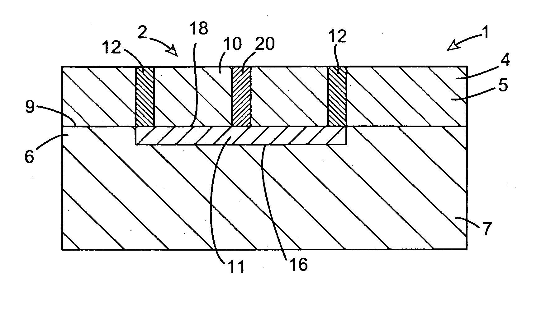
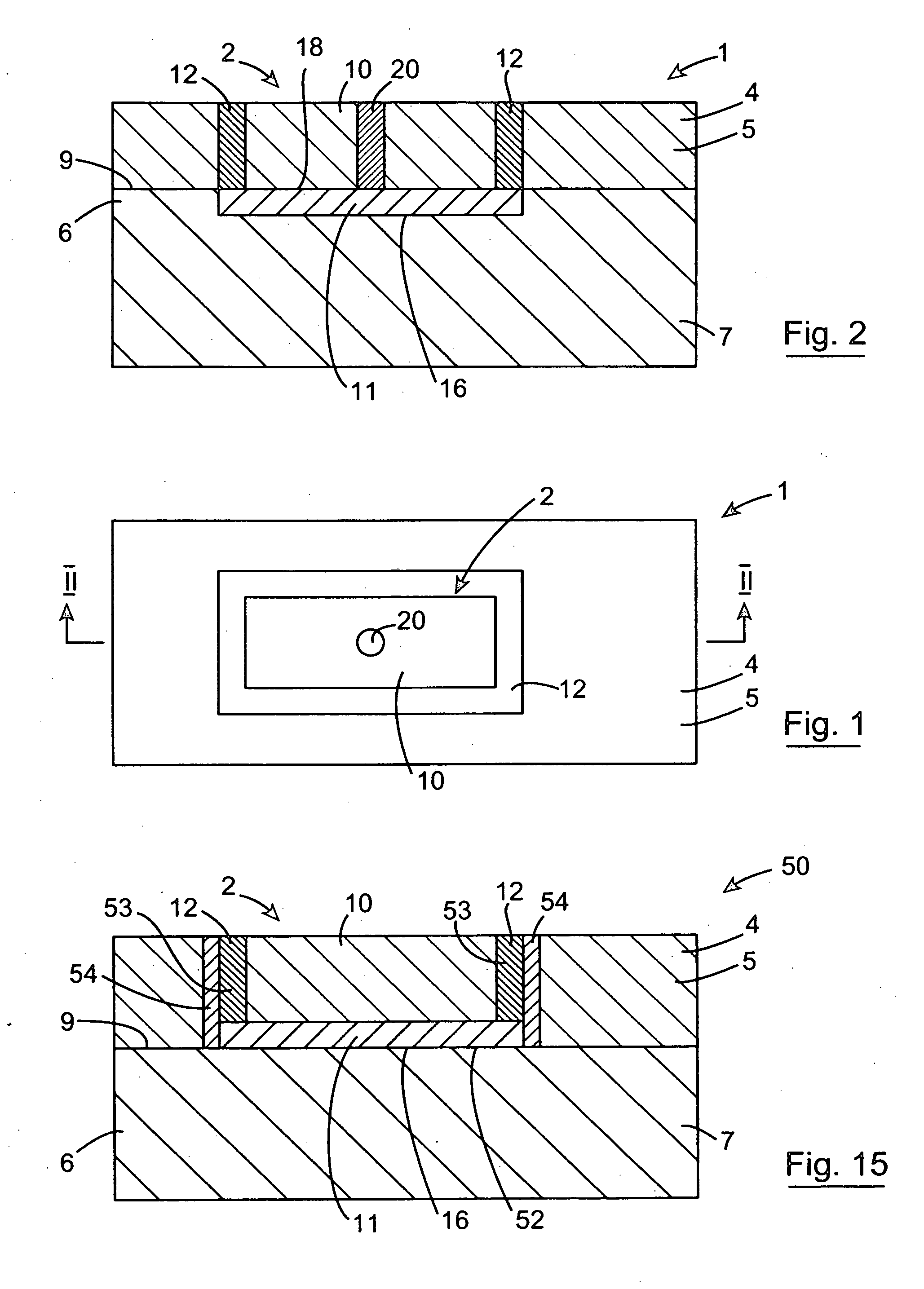
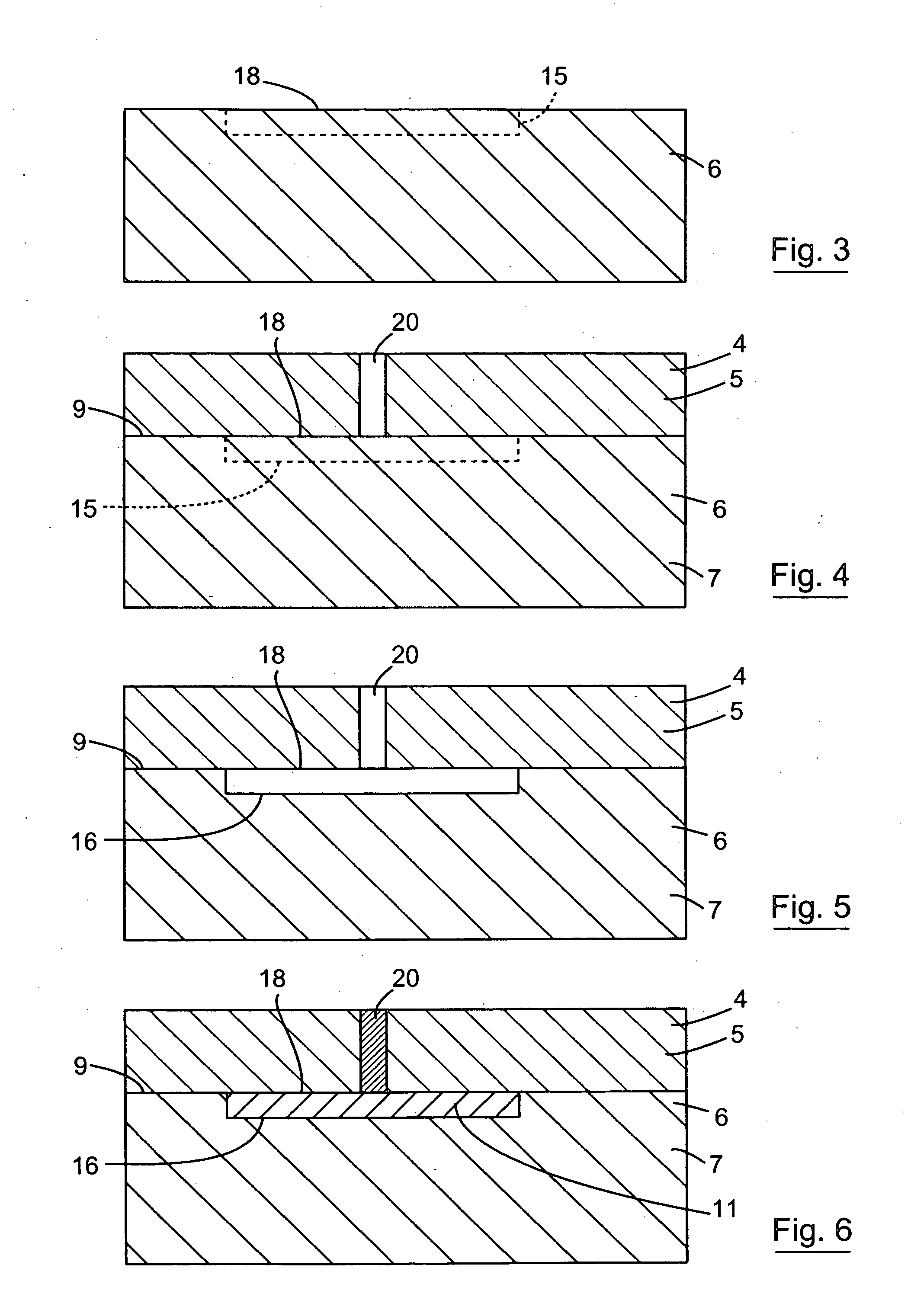
[0084] Referring to the drawings and initially to FIGS. 1 to 6, there is illustrated a semiconductor substrate according to the invention, indicated generally by the reference numeral 1, which comprises a silicon-on-insulator (SOI) 2 formed therein. The semiconductor substrate 1 is formed by a method which is also according to the invention. The semiconductor substrate 1 comprises a pair of semiconductor wafers, namely, a first wafer 4 which forms a device layer 5 of the semiconductor substrate 1 and a second wafer 6 which forms a handle layer 7. The first and second wafers 4 and 6 are of single crystal silicon and are directly bonded together by high temperature anneal bonding along a bond interface 9. The SOI 2 is formed by a portion 10 of the first wafer 4 beneath which a laterally extending buried insulating layer 11 is formed as will be described below. An electrical isolation trench 12 extends around the portion 10 of the first wafer 4 which forms the partial SOI 2 for insulat...


PUM


Abstract

A semiconductor substrate (1) comprising an SOI (2) formed therein. The semiconductor substrate (1) comprises first and second wafers (4,6) which are directly bonded together along a bond interface (9). Prior to bonding the wafers (4,6), a portion (15) of the second wafer (6) is ion implanted to form a p+ region for facilitating selective etching thereof to form a buried cavity (16), in which a buried insulating layer is subsequently formed under a portion (10) of the first wafer (4) for forming the SOI (2). After bonding of the first and second wafers (4,6) a communicating opening (20) is etched through the first wafer (4) to the bond interface (9), and the selectively etchable portion (15) is etched through the communicating opening (20) to form the buried cavity (16). The buried cavity (16) is then filled with deposited oxide to form the buried insulating layer (11). An isolation trench (12) is formed through the first wafer (4) to the buried insulating layer (11) around the portion (10) for isolating the SOI (2) from the remainder of the first wafer (4).

Description

FIELD OF THE INVENTION [0001] The present invention relates to a method for forming a buried cavity in a semiconductor substrate, and to a method for forming an SOI in the semiconductor substrate. The invention also relates to a semiconductor substrate having a buried cavity formed therein, and to a semiconductor substrate having an SOI formed therein. BACKGROUND OF THE INVENTION [0002] Semiconductor substrates formed by direct bonded semiconductor wafers, for example, direct bonded single crystal silicon wafers are commonly used in the manufacture of power devices such as PIN diodes, insulated gate bipolar transistors, as well as photo-detectors, and micro-electromechanical systems (MEMS). The advantage of forming PIN diodes, insulated gate bipolar transistors, photo-detectors and other such semiconductor electronic devices in directly bonded silicon wafers is that it avoids the need to form a deposited silicon (epitaxy) layer on a silicon wafer in which the power devices are to be...

Claims


Application Information

Patent Timeline
Patent Type & Authority Applications(United States)
IPC IPC(8): H01L21/30H01L21/306H01L21/311H01L21/762
CPCH01L21/76264H01L21/30604
Inventor NEVIN, WILLIAM ANDREWMCCANN, PAUL DAMIEN
Owner ANALOG DEVICES INC
Why Eureka
Try Eureka