Sectional field effect devices and method of fabrication

a technology of field effect devices and fabrication methods, applied in the field of integrated circuits and their manufacturing, can solve the problems of large difficulty in maintaining performance improvement of devices of deeply submicron generation, visible limits to straightforward downsizing, and complex technology, and achieve excellent layout density

Active Publication Date: 2005-06-16
GLOBALFOUNDRIES US INC
View PDF11 Cites 132 Cited by
  • Summary
  • Abstract
  • Description
  • Claims
  • Application Information

AI Technical Summary

Benefits of technology

[0006] The invention teaches the method for fabricating such structures. One uses a combination of sidewalls and an insulator layer, which insulator layer is disposed over a SOI layer, to create a formation of walls standing on the patterned insulator layer. This formation is then transferred, with the aid of several etching steps, into the SOI layer. Where the wall was standing there will be Fins formed in the SOI

Problems solved by technology

As FET (Field-Effect-Transistor) devices are being scaled down, the technology becomes more complex.
There is great difficulty in maintaining performance improvements in devices of deeply submicron generations.
However, there are visible limits to straightforward downsizing as, among other issues, short-channel effects (SCE) become a major problem when devices are scaled down to th

Method used


Image

  • Sectional field effect devices and method of fabrication
  • Sectional field effect devices and method of fabrication
  • Sectional field effect devices and method of fabrication

Examples


Embodiment Construction

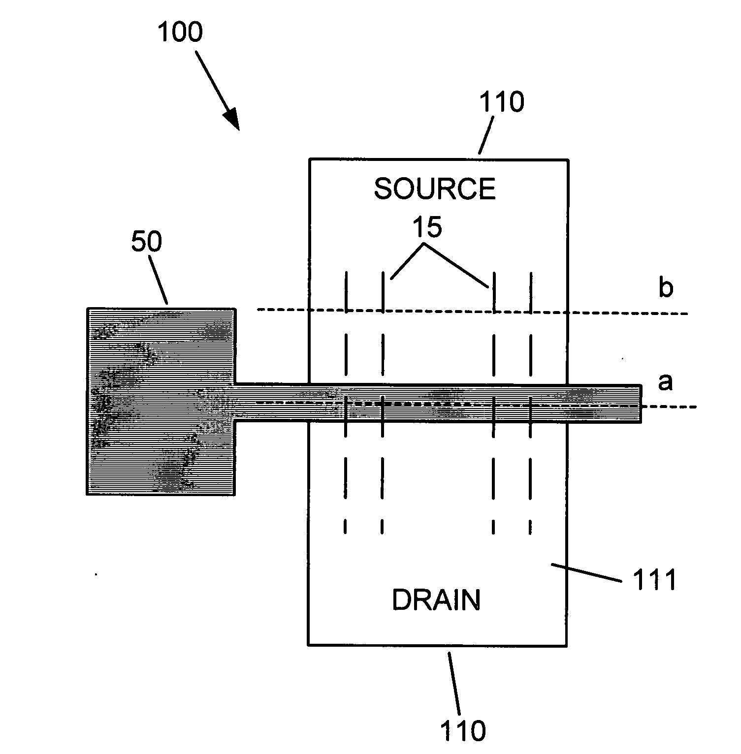
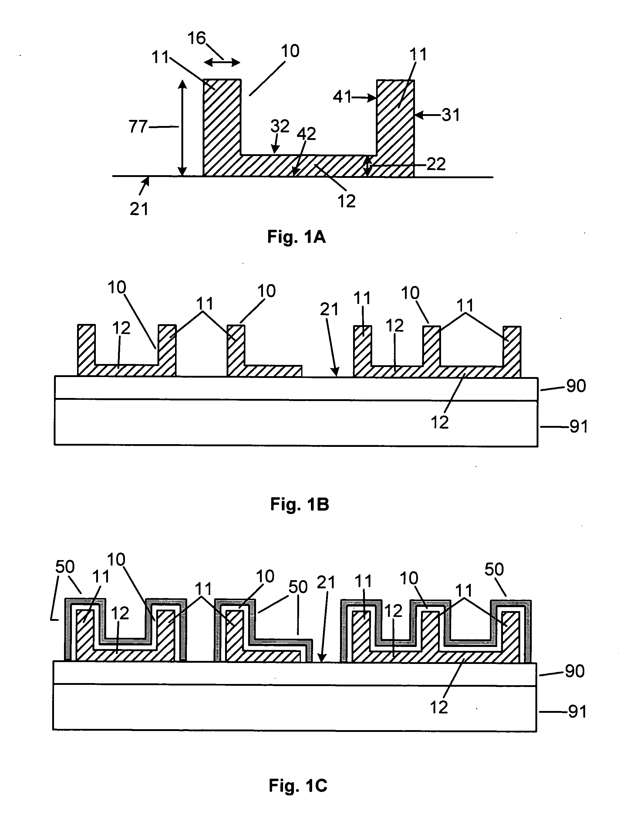
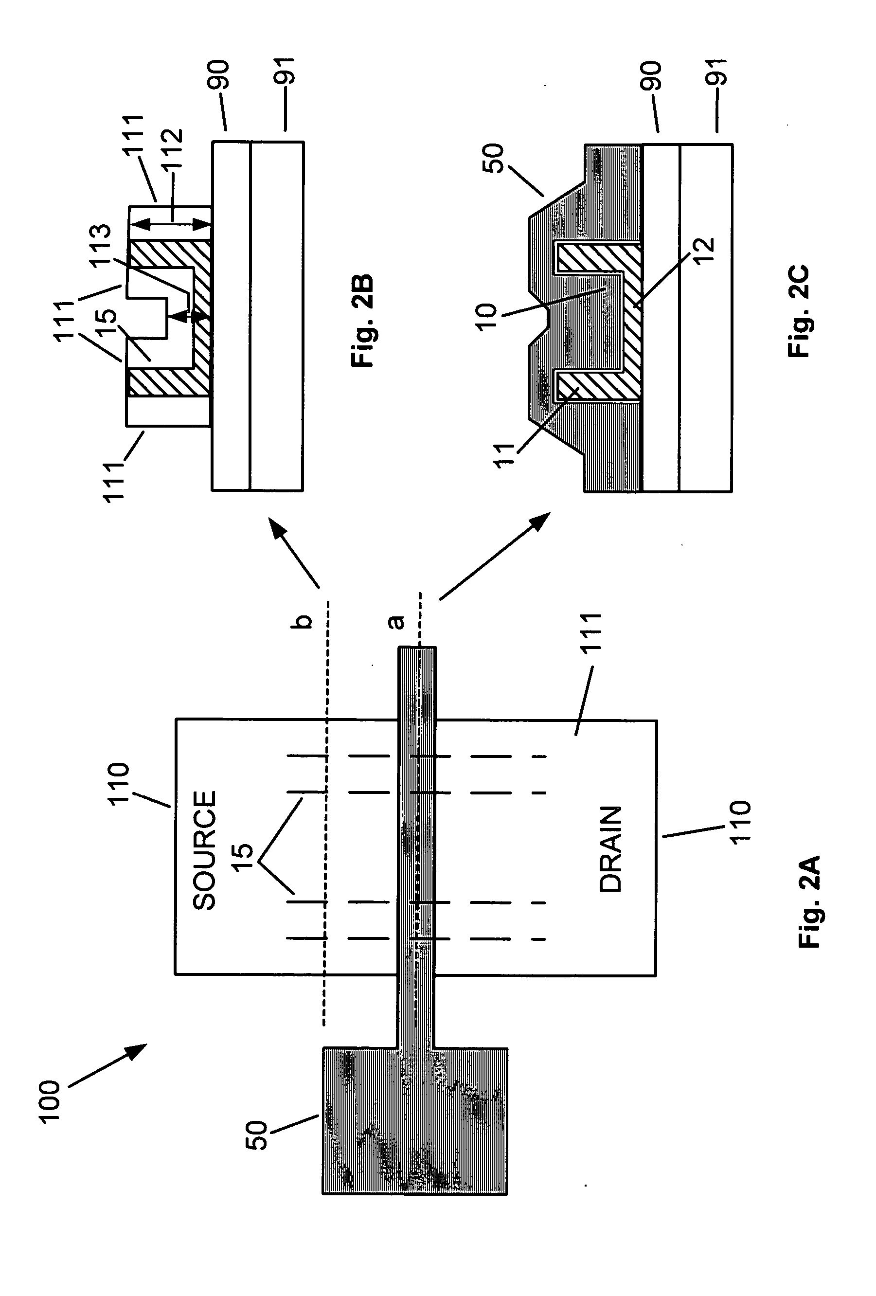
[0012]FIG. 1 shows schematic cross sectional views of the body regions of various embodiments of sectional FETs. In general, a Field-Effect-Transistor (FET) is a device where the current flow is controlled by a gate electrode between two parts of the device, the source and the drain. The gate electrode exerts its control with a field over the body of the device. The body is between the source and the drain and the gate electrode engages the body over a surface, or face. The gate electrode typically, but not necessarily, is separated form the face, or faces, of the body by a gate dielectric. The body of the FET is a crystalline semiconductor, where the face upon which the gate electrode exerts its field can form a conductive channel between the source and the drain. The common FET as known in the art has a single horizontal body section engaged by the gate electrode. The present disclosure contemplates FET devices with multiple body sections, having both horizontally oriented and ver...


PUM


Abstract

A field effect device is disclosed which has a body formed of a crystalline semiconductor material and has at least one vertically oriented section and at least one horizontally oriented section. The device is produced in SOI technology by fabricating first a formation of the device in masking insulators, and then transferring this formation through several etching steps into the SOI layer. The segmented field effect device combines FinFET, or fully depleted silicon-on-insulator FETs, type devices with fully depleted planar devices. This combination allows device width control with FinFET type devices. The segmented field effect device gives high current drive for a given layout area. The segmented field effect devices allow for the fabrication of high performance processors.

Description

FIELD OF THE INVENTION [0001] The present invention relates to the field of integrated circuits and their manufacturing. More particularly, the present invention relates to field effect semiconductor devices with the device body having horizontally oriented and vertically oriented sections. BACKGROUND OF THE INVENTION [0002] Today's integrated circuits include a vast number of devices. Smaller devices are key to enhance performance and to improve reliability. As FET (Field-Effect-Transistor) devices are being scaled down, the technology becomes more complex. There is great difficulty in maintaining performance improvements in devices of deeply submicron generations. Several avenues are being explored for keeping device performance improvements on track Along the path of seeking ever higher device performances, downscaling of FET devices is the established guiding principle for current CMOS device technology. However, there are visible limits to straightforward downsizing as, among o...

Claims


Application Information

Patent Timeline
IPC IPC(8): H01L21/335H01L29/812H01L21/336H01L21/338H01L29/423H01L29/786
CPCH01L29/42384H01L29/785H01L29/66795H01L21/18
Inventor ZHANG, YINGDORIS, BRUCE B.KANARSKY, THOMAS SAFRONIEONG, MEIKEIKEDZIERSKI, JAKUB TADEUSZ
Owner GLOBALFOUNDRIES US INC
Why Eureka
Try Eureka