

Organic light-emitting device
- Summary
- Abstract
- Description
- Claims
- Application Information
AI Technical Summary
Benefits of technology
Problems solved by technology
Method used
Image

Examples
example 1
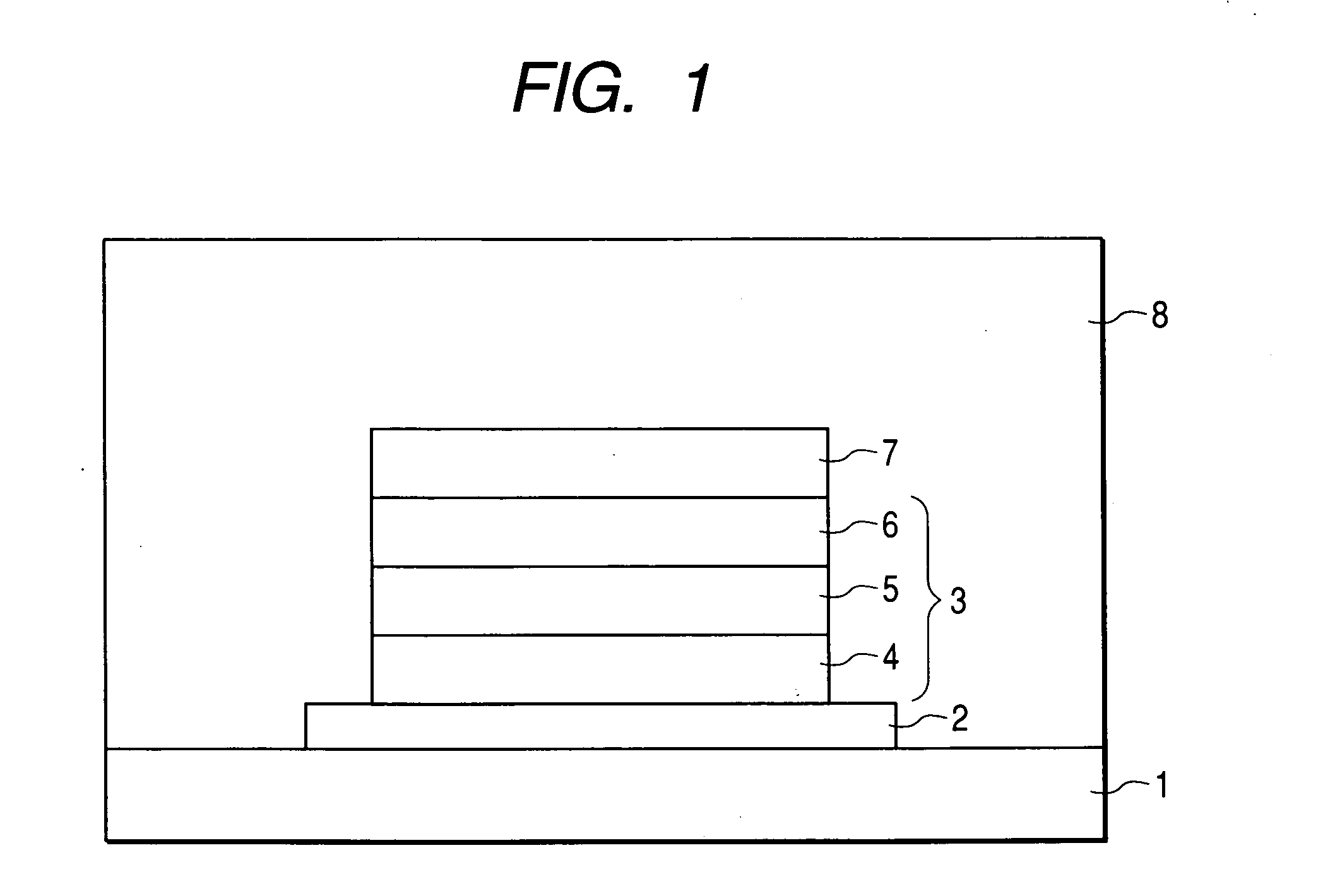
[0052] The organic light-emitting device shown in FIG. 1 was formed as described below.
[0053] A film of indium tin oxide (ITO) as an anode 2 was formed to have a thickness of 120 nm on a glass substrate 1 by means of sputtering. The substrate with the film was subjected to ultrasonic cleaning with acetone and isopropyl alcohol (IPA) sequentially. Then, the substrate with the film was subjected to boiling and cleaning with IPA and dried. After that, the substrate with the film was subjected to UV / ozone cleaning, and was used as a transparent conductive support substrate.
[0054] A solution having a concentration of 0.1 wt % of the organic compound D that had not been subjected to sublimation purification was dropped onto the ITO electrode. Then, the dropped solution was subjected to spin coating at 500 RPM for 10 seconds and then at 1,000 RPM for 1 minute to form a film. After that, the film was dried in a vacuum oven at 80° C. for 10 minutes to completely remove the solvent in the t...
example 2
[0061] An organic light-emitting device was produced in the same manner as in Example 1 except the following points. First, the hole-transporting layer 4 was formed by using the organic compound D that had been subjected to sublimation purification. Second, the organic compound C that had been subjected to sublimation purification as the host material of the organic luminescent layer 5 and the organic compound A′ that had been subjected to sublimation purification as the dopant material were co-deposited (the film forming rate at the time of co-deposition was adjusted to 0.5 nm / sec for the host material and to 0.1 nm / sec for the dopant material). Third, the electron-transporting layer 6 was formed by using the organic compound C that had been subjected to sublimation purification.
[0062] The obtained organic light-emitting device had an emission chromaticity of green (0.28, 0.63) and a luminance of 150 cd / m2 at 3.7 V and 300 cd / m2 at 4.0 V.
[0063] In addition, when a voltage was app...
PUM
| Property | Measurement | Unit |
|---|---|---|
| Durability | aaaaa | aaaaa |
| Luminescence | aaaaa | aaaaa |
Abstract
Description
Claims
Application Information