

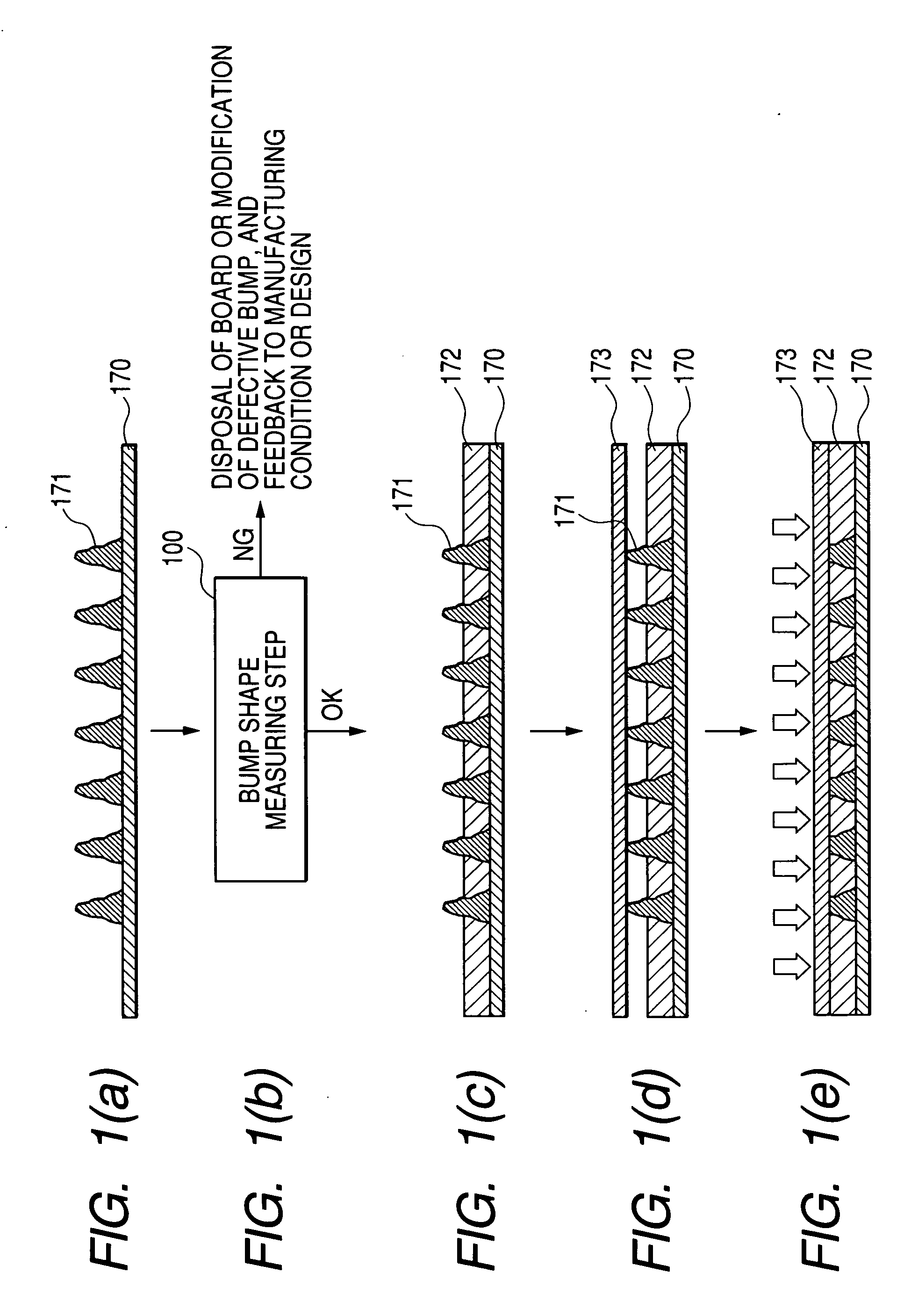
Method and apparatus for measuring shape of bumps
a technology of bumps and measuring methods, applied in the direction of electrical connection formation of printed elements, instruments, image enhancement, etc., can solve the problems of inadequate consideration, high density and low cost of connection methods using bumps, etc., and achieve the effect of simplifying the configuration of the apparatus, high accuracy and high speed
- Summary
- Abstract
- Description
- Claims
- Application Information
AI Technical Summary
Benefits of technology
Problems solved by technology
Method used
Image

Examples
first embodiment
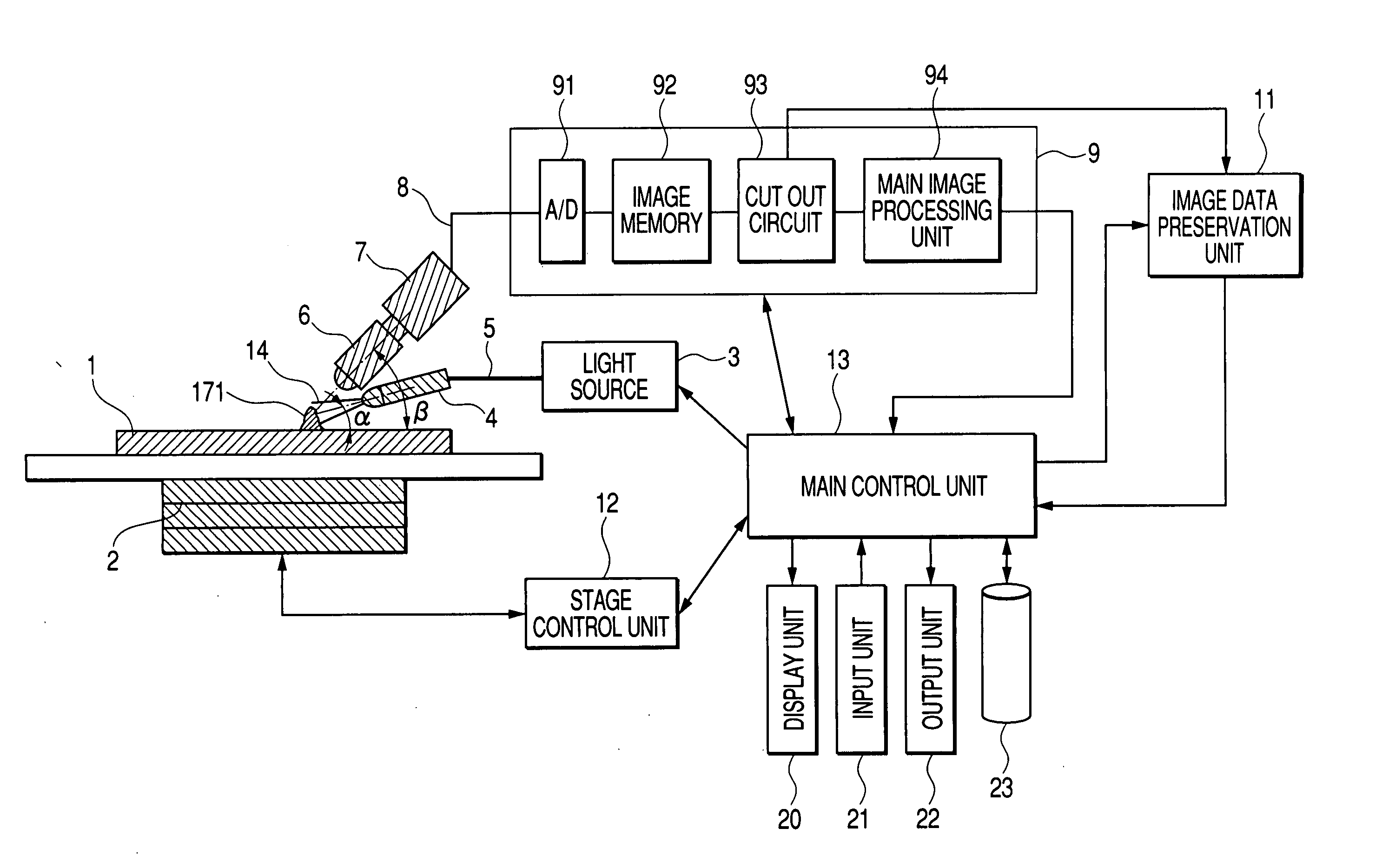
[0050] Next, the bump shape measuring apparatus according to the present invention for use in the bump shape measuring step 100 is described.
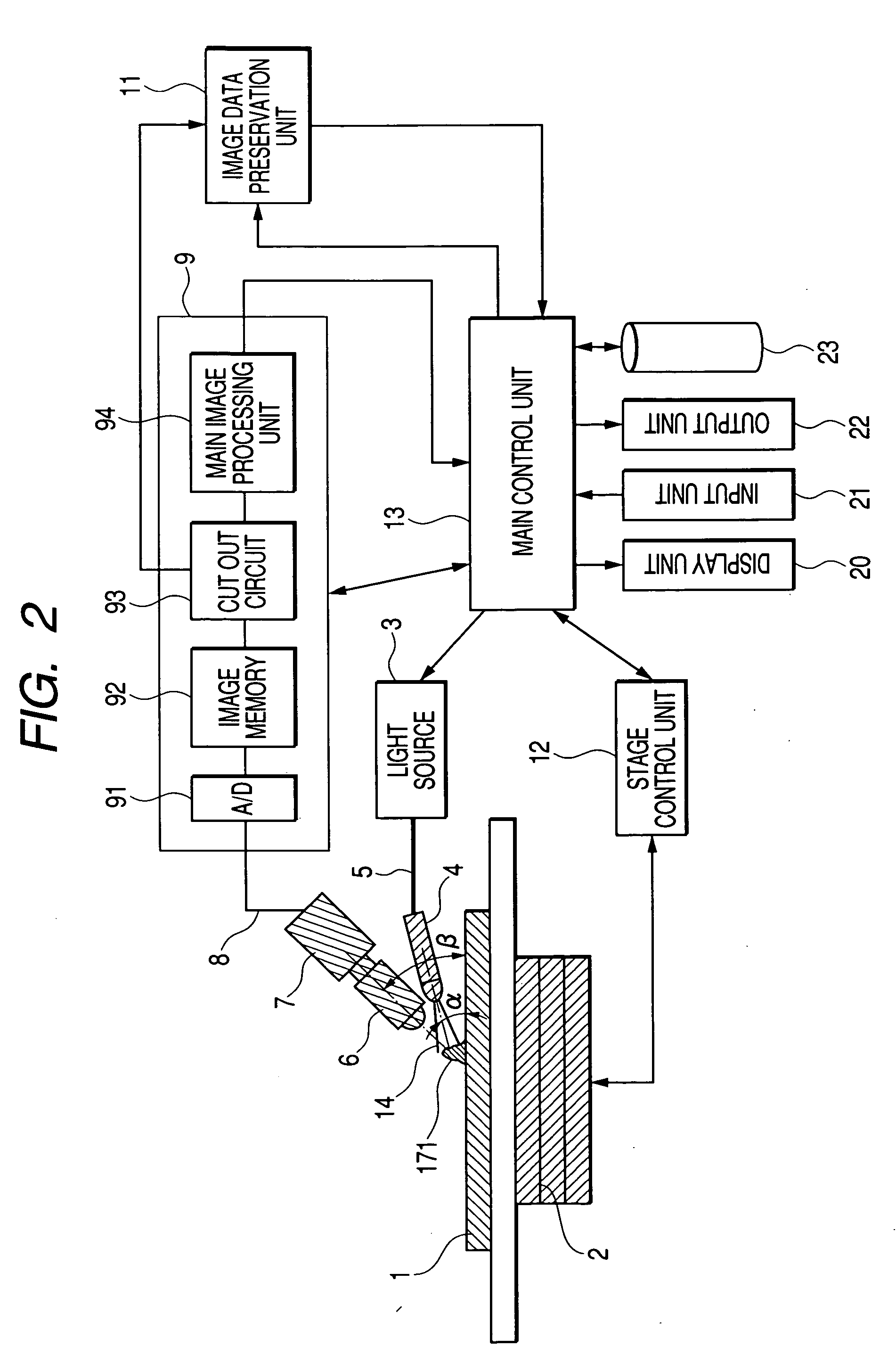
[0051]FIG. 2 is a configuration diagram showing a first embodiment of the bump shape measuring apparatus according to the present invention.
[0052] A printed board (board) 1 formed with thereon a plurality of bumps 171 to be measured is absorbed and mounted to a stage 2 movable to three directions of X, Y and Z. The reason why the stage 2 absorbs and holds the printed board 1 as described above is to eliminate the warpage of the printed board 1. Thus, the warpage is eliminated. In addition, the height of the bumps 171 is about 200 μm therefore, an automatic focusing control system of a condenser lens 6 for a surface of the printed board 1 need not be provided. Of course, when the automatic focusing control system is provided, the same bump image can be formed on an image detection camera 7 using the condenser lens 6 even if a thickness of the p...
second embodiment
[0088] How to use the second embodiment is described by referring to FIG. 15. The position and shape of the bump 171 of the printed board 1 having bumps to be measured mounted thereon are measured by the image processing unit 9 and the main control unit 13, based on the image signal 8 detected by the linear sensor cameras 7; 704 and 706; and the linear sensor devices 902 and 903. Further, the position and shape of the through-hole 180 of the multilayer printed board 10 having holes formed thereon are measured by the image processing unit 9 and the main control unit 13, based on the image signal 18 obtained by the detection camera 15. The detection camera 15 detects the position and shape of the through-hole 180 in the form of an image signal composed of a dark section indicating a circular hole part and a bright section indicating a circumference thereof. The main image processing unit 94 projects, for example, an image signal in the region near the hole (it may be cut out for each ...
PUM
 Abstract
Description
Claims
Application Information