P and N contact pad layout designs of GaN based LEDs for flip chip packaging

a technology of flip chip and contact pad, which is applied in the direction of basic electric elements, electrical equipment, semiconductor devices, etc., can solve the problems of contact pad blocking the emitted light, heat dissipation problem, and current crowding effect being one of the primary limiting factors, so as to increase the current density, and efficient use of light-emitting materials

Inactive Publication Date: 2005-06-23
PENG HUI +1
View PDF6 Cites 31 Cited by
  • Summary
  • Abstract
  • Description
  • Claims
  • Application Information

AI Technical Summary

Benefits of technology

[0011] The second object and advantage is to provide new P and N contact pad layout designs for efficiently utilizing light emitting material of active layer.
[0012] The third object and advantage is to provide new P and N contact pad layout designs for uniformly distributing the current and, thus increasing the current density.
[0013] The fourth object and advantage is to provide new P and N contact pad layout designs for more uniform and bright surface emission.
[0014] The fi

Problems solved by technology

There are three major issues for the LED design and manufacture: the current crowding effect, the heat dissipation problem, and the problem of a large contact pad blocking the emitted light.
The current crowding effect is one of the primary limiting factors in LED die design and manufacture.
It results in an unstable luminous flux output with drifting bright and dim spots on the LED chip and it preve

Method used


Image

  • P and N contact pad layout designs of GaN based LEDs for flip chip packaging
  • P and N contact pad layout designs of GaN based LEDs for flip chip packaging
  • P and N contact pad layout designs of GaN based LEDs for flip chip packaging

Examples


Embodiment Construction

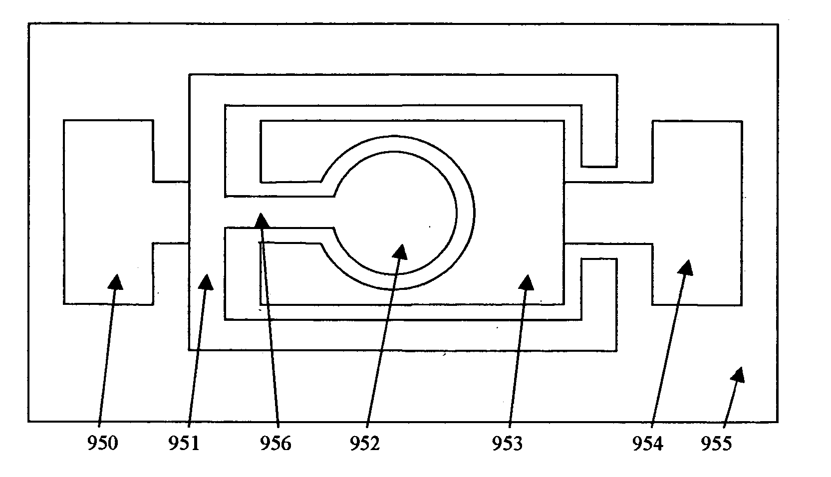
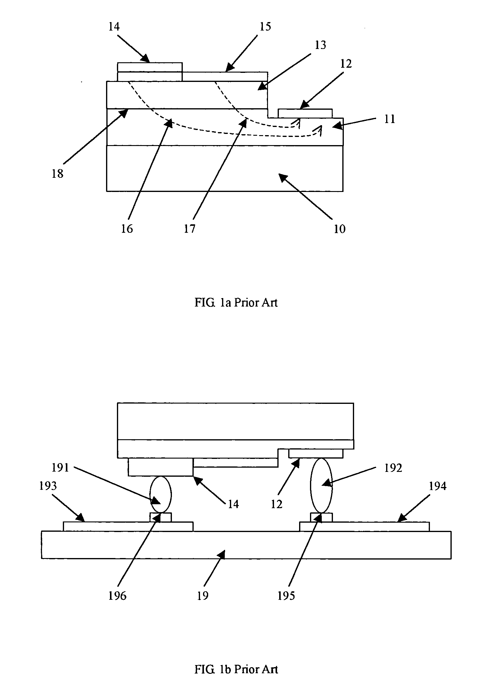
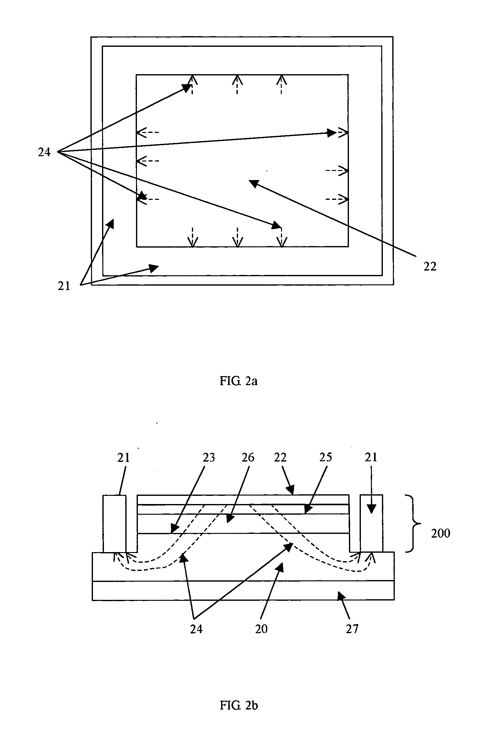
[0047] With the application of the flip chip packaging process to LEDs layout design and manufacture, the conventional principles for P and N contact pad layout designs of GaN based LEDs need to be modified. The quantity, sizes, shapes, and positions of P and N contact pads all become useful variables for optimizing the contact pad layout designs. The designs of P and N contact pad layout of LEDs can be focused on certain issues such as the current crowding effect and the utilization of the light emitting semiconductor material of the active region.

[0048] The P contact pad can be designed with larger area and different shapes. The larger contact area will reduce the contact resistance and therefore the heat generation, because the contact resistance is inversely proportional to the contact area. Multiple P and N contact pads can be integrated into one LED die.

[0049] While embodiments of the present invention will be described below, those skilled in the art will recognize that oth...


PUM


Abstract

Based on the unique properties of the flip chip packaging process and GaN based LEDs with transparent substrates, new principles and methods for designing the layout of P contact pads and N contact pads are disclosed. The new designs of the present invention drastically increase the light extraction efficiency of LEDs by reducing the current crowding effect, increasing the uniformity of the spreading current in the active layer, and utilizing most of the available light emitting semiconductor material of the active layer. The present invention combined with the flip chip packaging process significantly improves the LEDs' heat dissipation.

Description

BACKGROUND OF THE INVENTION [0001] 1. Field of the Invention [0002] The present invention relates to new P and N contact pads layout designs of GaN based Light Emitting Diodes (LEDs) with transparent substrates for flip chip packaging and a new method of manufacturing the same. This invention drastically increases light extraction efficiency of GaN based LEDs. This invention makes a major improvement on the LED's heat dissipation. [0003] 2. Prior Art [0004] There are three major issues for the LED design and manufacture: the current crowding effect, the heat dissipation problem, and the problem of a large contact pad blocking the emitted light. [0005] Given the common LED die designs, the electrical current can't be evenly spread through the LED active layer or most of the current concentrates at a portion of the active layer (the current crowding effect). The current crowding effect is one of the primary limiting factors in LED die design and manufacture. It results in an unstable ...

Claims


Application Information

Patent Timeline
IPC IPC(8): H01L29/22H01L33/08H01L33/20H01L33/38H01L33/62
CPCH01L33/08H01L33/20H01L2924/12041H01L33/62H01L2224/16H01L33/382H01L24/05H01L24/06H01L24/16H01L2224/05568H01L2224/05573H01L2224/0603H01L2224/06102H01L2224/1703H01L2924/00014H01L2224/05599
Inventor PENG, HUIPENG, GANG GRANT
Owner PENG HUI
Why Eureka
Try Eureka