Apparatus for pulse testing a MRAM device and method therefore

a pulse and mram technology, applied in semiconductor devices, digital storage, instruments, etc., can solve the problems of memory failure, slow program and erase times, and limited ability to write or store charge in floating oxides

Inactive Publication Date: 2005-06-23
EVERSPIN TECHNOLOGIES
View PDF9 Cites 10 Cited by
  • Summary
  • Abstract
  • Description
  • Claims
  • Application Information

AI Technical Summary

Problems solved by technology

Moreover, they have slow program and erase times. The ability to write or store charge in the floating oxide is limited to a finite number of times that can be exceeded depending on the application.
Memory failure occurs if the maximum number of writes is exceeded.
FLASH memory is limited for high density applications because it cannot be continually scaled to smaller dimensions due to...

Method used


Image

  • Apparatus for pulse testing a MRAM device and method therefore
  • Apparatus for pulse testing a MRAM device and method therefore
  • Apparatus for pulse testing a MRAM device and method therefore

Examples


Embodiment Construction

[0015] The following detailed description is merely exemplary in nature and is not intended to limit the invention or the application and uses of the invention. Furthermore, there is no intention to be bound by any expressed or implied theory presented in the preceding technical field, background, brief summary or the following detailed description.

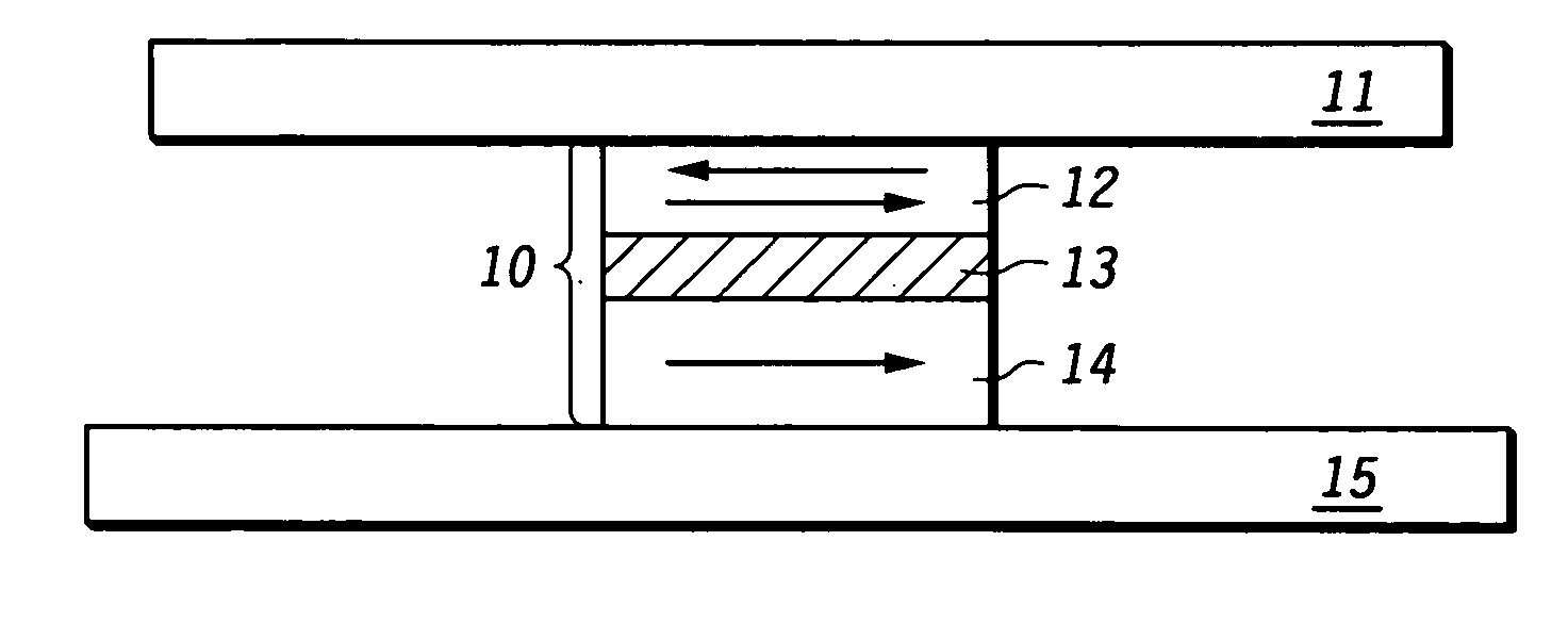
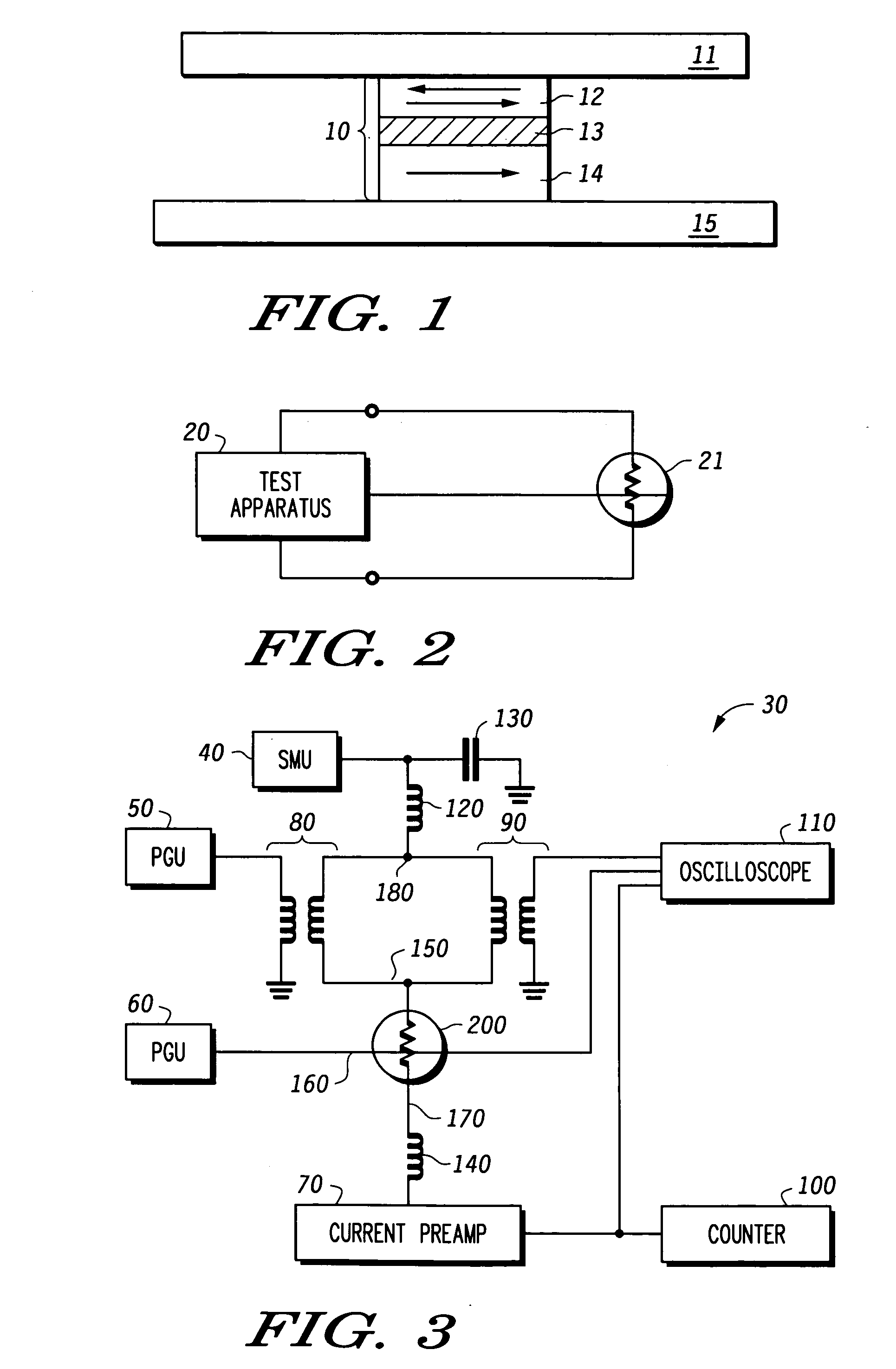
[0016] A typical architecture of a magnetoresistive random access memory (MRAM) comprises an array of magnetic tunnel junction (MTJ) cells and CMOS circuitry to read and write to the memory array. Each MTJ cell is located at a unique intersection of a particular bit line and digit line in the memory array. The bit lines and digit lines respectively correspond to column and row lines of more common memory types. Programming of a MTJ cell is achieved by passing current pulses through the bit line and the digit line that intersect at the MTJ cell. The magnetic fields generated by the current pulses in the bit line and the digit line are cou...


PUM


Abstract

Methods and apparatus are provided for testing a magnetoresistive random access memory (MRAM). A magnetoresistive tunnel junction (MTJ) has a first terminal, a second terminal, and a third terminal. A source measuring unit is coupled to a first terminal of a MTJ to provide DC biasing. A current preamp has an input coupled to a third terminal of the MTJ for receiving current corresponding to a resistance of the MTJ. A pulse generator is AC coupled to the MTJ for programming the MTJ. A method of insitu testing a MTJ in a manufacturing environment uses a probe station coupled to the MTJ. A probe station couples to the MTJ. The MTJ is DC biased for generating a current corresponding to the logic level stored in the MTJ. A pulse for programming the MTJ is AC coupled to the MTJ.

Description

TECHNICAL FIELD OF THE INVENTION [0001] The present invention generally relates to testing of semiconductor integrated circuits, and more particularly relates to testing magnetoresistive random access memories (NRAMs). BACKGROUND OF THE INVENTION [0002] Memories comprise one of the largest markets for semiconductor integrated circuits. In general, a memory is a storage device that retains information or data that can be output when needed. Memory devices are often characterized under such names as high speed, high density, or non-volatile memories. A high speed memory, as its name implies is a device having extremely fast read / write times that are useful in situations where data transfer rates are critical. A high density memory has a substantial memory size for large storage capability. The most common high density solid state memory is a dynamic random access memory (DRAM). A non-volatile memory is a memory that retains information even when power is removed and is thereby a perma...

Claims


Application Information

Patent Timeline
IPC IPC(8): G11C29/50G11C29/56H01L31/072
CPCG11C11/16G11C29/56G11C29/50
Inventor DEHERRERA, MARKRIZZO, NICHOLAS
Owner EVERSPIN TECHNOLOGIES
Why Eureka
Try Eureka