Semiconductor device and driving method thereof

a technology of electromagnetic field and driving method, applied in the direction of mechanical actuation of burglar alarms, pulse techniques, instruments, etc., can solve problems such as circuit elements of broken circuits, and achieve the effect of preventing element breakdown

Inactive Publication Date: 2005-06-23
SEMICON ENERGY LAB CO LTD
View PDF5 Cites 61 Cited by
  • Summary
  • Abstract
  • Description
  • Claims
  • Application Information

AI Technical Summary

Benefits of technology

[0025] According to the invention, a semiconductor device and a driving method thereof can be provided without the need of a special process, whereby an element breakdown can be prevented even when a high electro

Problems solved by technology

Otherwise, circuit elements thereof might be broken

Method used


Image

  • Semiconductor device and driving method thereof
  • Semiconductor device and driving method thereof
  • Semiconductor device and driving method thereof

Examples


embodiment 1

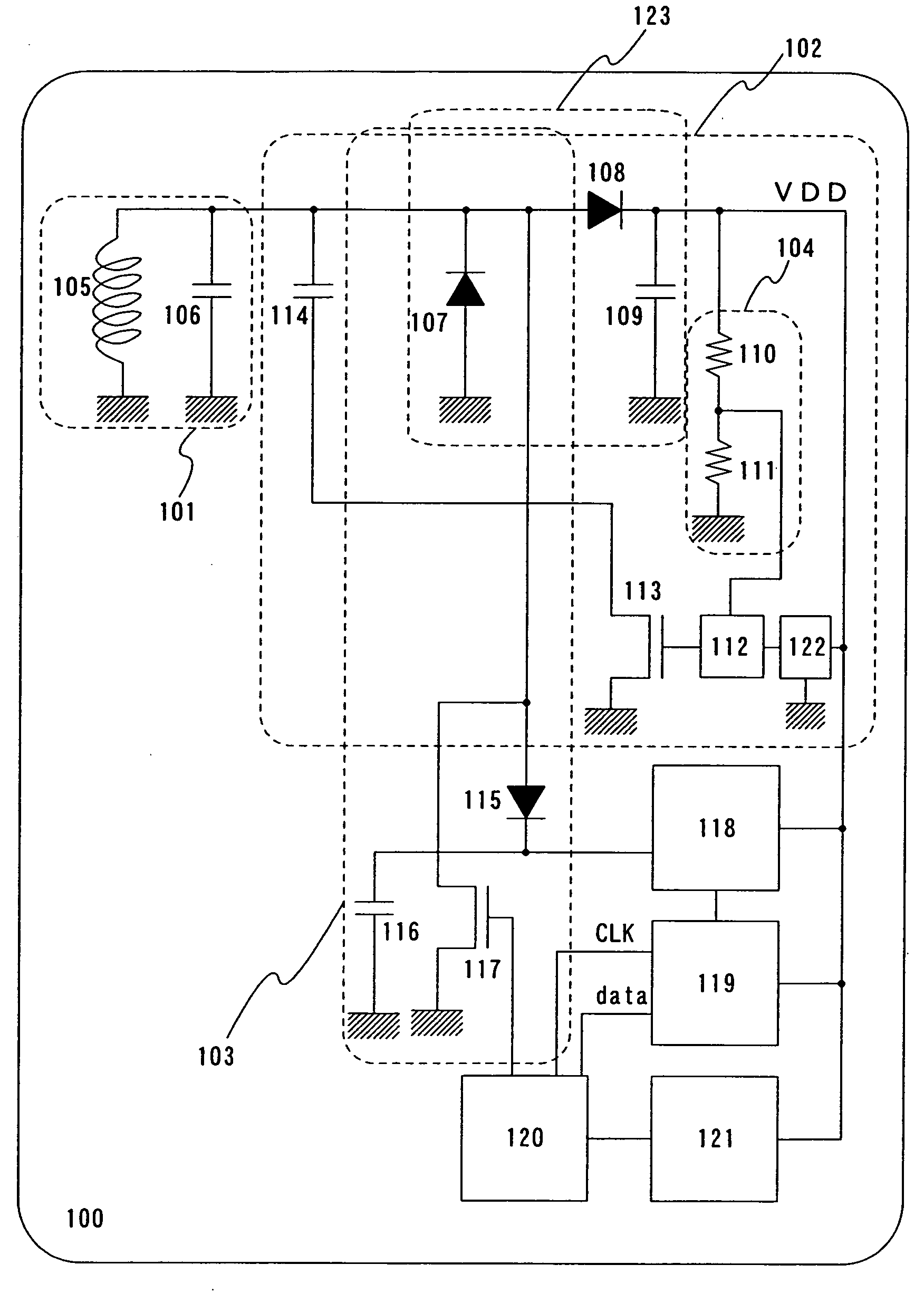
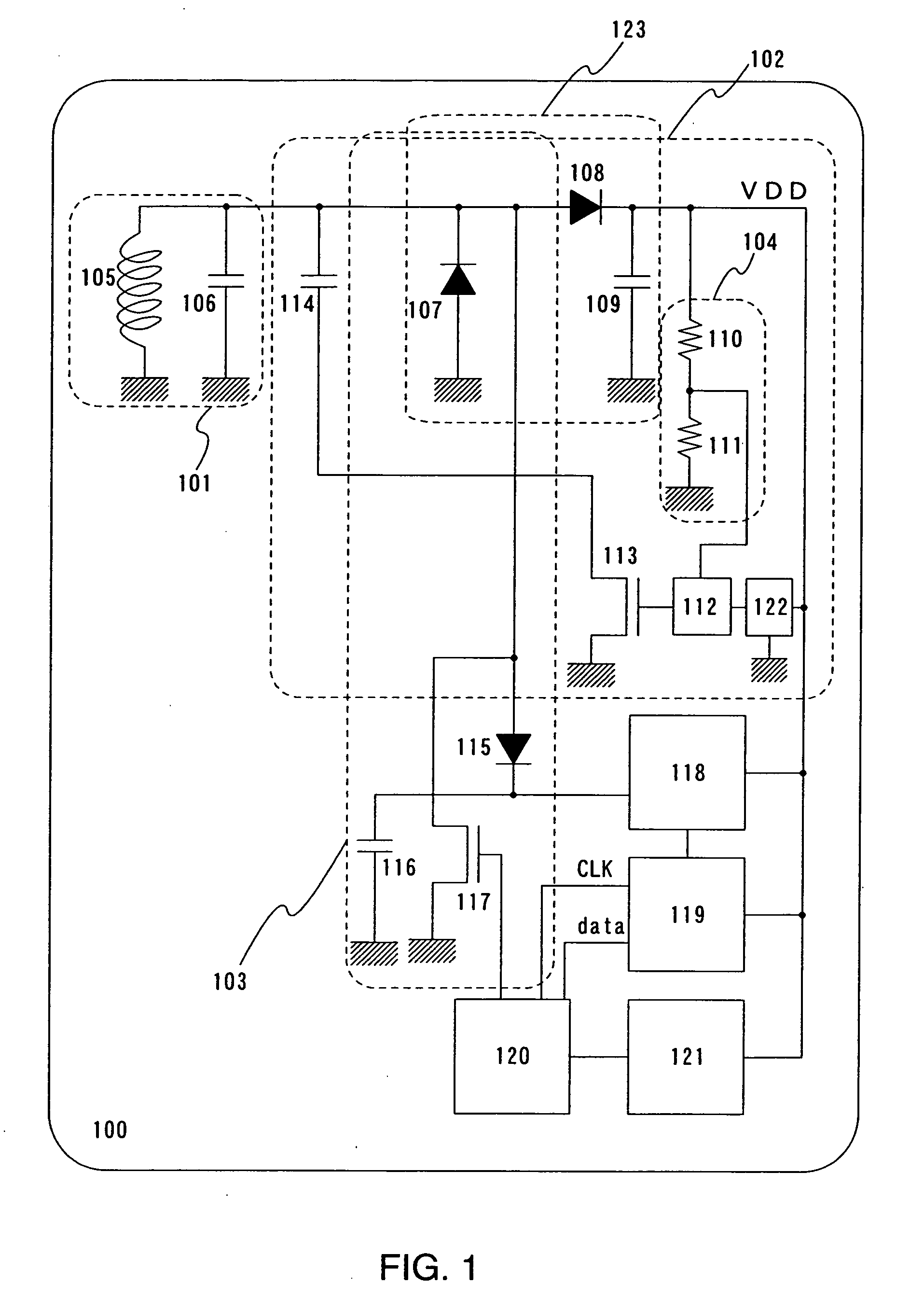
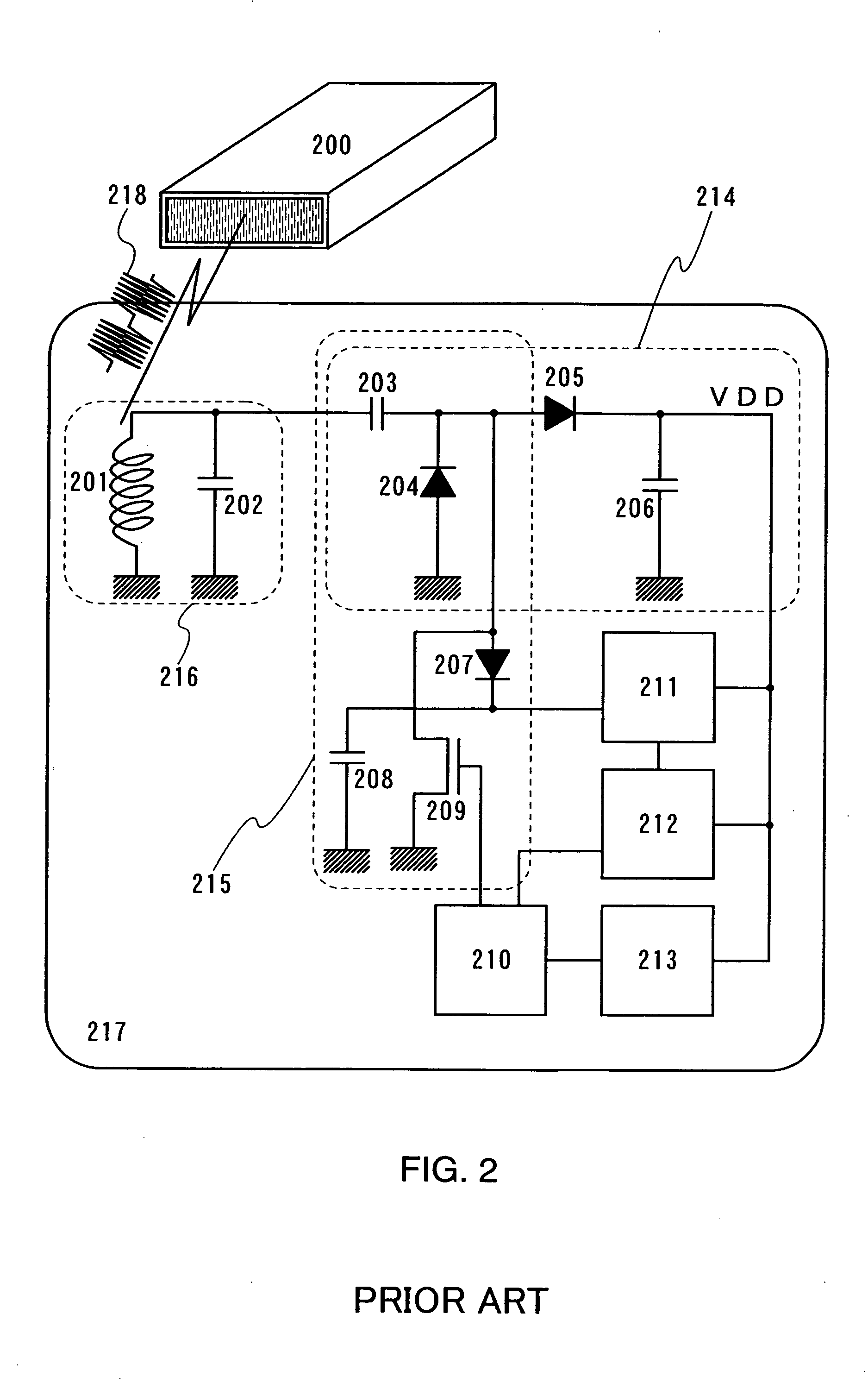
[0073] Referring to FIG. 22, description is made on a power supply circuit portion which has a different mode from the power supply circuit 102 shown in FIG. 1. FIG. 22 illustrates a circuit comprising a first antenna circuit 1801, a second antenna circuit 1802, a first converter circuit 1803, a second converter circuit 1804, a comparator circuit 1805, a switch element 1806 and a capacitor 1807. The second antenna circuit 1802 is configured so as to generate a lower voltage than the voltage generated in the first antenna circuit 1801. For example, the area occupied by an antenna in the second antenna circuit 1802 can be designed smaller than that in the first antenna circuit 1801. Alternatively, the antenna or a capacitor in the second antenna circuit 1802 may have different configurations from that of the first antenna circuit 1801 to obtain a slightly shifted resonance frequency. Though not shown, a monitor circuit as shown in FIG. 1 may be provided between the converter circuits ...

embodiment 2

[0077] Description is made now on the method for integrally forming TFTs which are used for the switch elements and diodes shown in embodiment mode over the same insulating substrate with reference to FIGS. 6A to 8. Note that N-channel TFTs and P-channel TFTs are taken as examples of semiconductor elements in this embodiment, however, semiconductor elements of the ID chip of the invention are not limited to them. In addition, the manufacturing method herein described is only an example, and the invention is not limited to such manufacturing method on an insulating substrate.

[0078] First, as shown in FIG. 6A, a base film 3001 formed of an insulating film such as a silicon oxide film, a silicon nitride film, a silicon oxynitride film is formed over a substrate 3000 formed of heat-resistant plastic or glass such as barium borosilicate glass and alumino borosilicate glass typified by Corning #7059 or #1737. For example, the base film 3001 has a lamination of a silicon oxynitride film 3...

embodiment 3

[0104] In this embodiment, description is made on the manufacturing method which is from the formation of an ID chip up to the transfer thereof to a flexible substrate with reference to FIGS. 9A and 9B and FIGS. 10A and 10B. Note that N-channel TFTs and P-channel TFTs are used as the semiconductor elements in this embodiment, however, the semiconductor elements of the ID chip of the invention are not limited to them. In addition, the manufacturing method on an insulating substrate described herein is only an example, and the invention is not limited to this.

[0105] In accordance with the manufacturing steps described in Embodiment 2, steps up to the formation of the first and second interlayer insulating films are completed as shown in FIG. 8. However in this embodiment, a metal oxide film 4021 is formed between the substrate 3000 and the base film 3001. The metal oxide film 4021 may be an oxide of W, TiN, WN, Mo and the like, or an oxide of alloys of such elements. The metal oxide ...


PUM


Abstract

There has been a problem in battryless RFID chips that a high voltage AC signal is generated when an antenna is exposed to a high electromagnetic field, and a DC voltage that is obtained through rectification of the AC signal becomes a high voltage accordingly. As a result, heat generation of a logic circuit and a clock generator circuit or element break down occur. The invention takes the following measures: a DC voltage generated through rectification of an AC signal is compared with a reference voltage in a comparator circuit, and a switch element is turned ON when the DC voltage becomes higher so as to add capacitance to an antenna circuit. Accordingly, resonance point of an antenna changes which in turn attenuates an AC signal generated in the antenna circuit, thereby suppressing a DC voltage.

Description

BACKGROUND OF THE INVENTION [0001] 1. Field of the Invention [0002] The present invention relates generally to a semiconductor device used for an IC card and an RFID (Radio Frequency Identification: contactless automatic identification technique by use of radio frequencies). In particular, the invention relates to a semiconductor device including a contactless IC card and an RFID chip which receive power and data from an external device in a contactless manner and transmit data to the external device, and a driving method thereof. [0003] Note that the RFID chip is used, for example, as a tag. In addition, the IC card is one type of the RFID chip. [0004] 2. Description of the Related Art [0005] In recent years, IC chips such as contactless ID chips using radio frequencies, namely those called RFID chips are attracting attentions, and achievement of higher performance thereof is expected. RFID chips have advantages that recoded data can be read out in a contactless manner, batteryless...

Claims


Application Information

Patent Timeline
IPC IPC(8): G06K19/07H03K19/00G06K19/077H01L27/08H04Q5/22
CPCG06K19/0723G06K19/0701H03K19/00
Inventor KOYAMA, JUNSAITO, TOSHIHIKO
Owner SEMICON ENERGY LAB CO LTD
Why Eureka
Try Eureka