Method of fabricating liquid crystal display device

a liquid crystal display and display panel technology, applied in semiconductor devices, instruments, optics, etc., can solve the problems of difficult to employ amorphous silicon tft as a high-resolution display panel, difficult to fabricate a process complex, and relatively slow response of amorphous silicon tft, etc., to achieve the effect of simplifying the fabricating process

Active Publication Date: 2005-06-23
LG DISPLAY CO LTD
View PDF7 Cites 40 Cited by
  • Summary
  • Abstract
  • Description
  • Claims
  • Application Information

AI Technical Summary

Benefits of technology

[0024] An object of the present invention is to provide a method of fabricating an LCD device having a simplified fabricating process.

Problems solved by technology

However, an amorphous silicon TFT has a relatively slow response due to its low charge mobility.
Thus, it is difficult to employ an amorphous silicon TFT as a high-resolution display panel that requires rapid response speeds or as a driving device for a gate driver and a data driver.
In addition, since each mask process includes a plurality of sub-processes, such as deposition, cleaning, photolithography, etching, photo-resist stripping, and inspection, the fabricating process is very complicated and increases fabrication costs.

Method used


Image

  • Method of fabricating liquid crystal display device
  • Method of fabricating liquid crystal display device
  • Method of fabricating liquid crystal display device

Examples


Embodiment Construction

[0053] Reference will now be made in detail to the preferred embodiments of the present invention, examples of which are illustrated in the accompanying drawing.

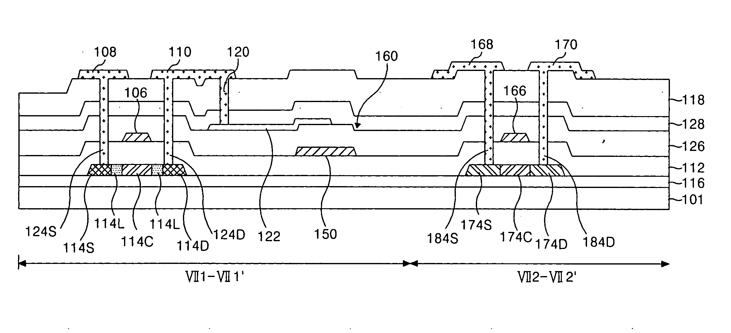
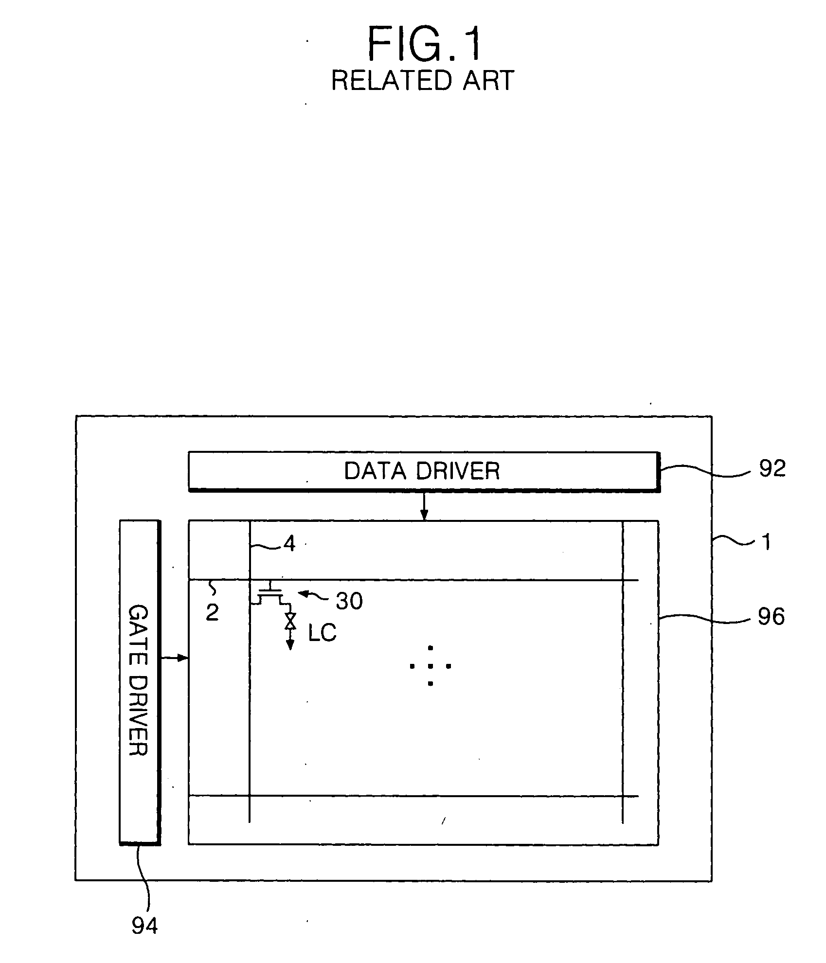
[0054]FIG. 6 is a plan view of an exemplary polycrystalline silicon LCD device according to the present invention, and FIG. 7 is a cross sectional view along VII1-VII1′ and VII2-VII2′ of FIG. 6 according to the present invention. In FIGS. 6 and 7, an LCD device may include a polycrystalline silicon type TFT that may include an image display part 196 having a matrix configuration of pixels, a data driver 192 for driving a data line 104 of the image display part 196, and a gate driver 194 for driving a gate line 102 of the image display part 196. The image display part 196 may include a gate line 102 and a data line 104 intersected and insulated from each other, an N-type TFT 130 of the image display part located at the intersection of the gate line 102 and the data line 104, a pixel electrode 122 formed at an area defined by...


PUM

PropertyMeasurementUnit
areaaaaaaaaaaa
insulatingaaaaaaaaaa
source areaaaaaaaaaaa

Abstract

A method of fabricating a liquid crystal display device includes forming a first active layer on a substrate, forming a first gate insulating film on the first active layer, forming a first gate electrode on the first gate insulating film, forming a first interlayer insulating layer on the first gate electrode, forming a pixel electrode on the first interlayer insulating layer, forming at least one insulating film to cover the pixel electrode, forming a first plurality of contact holes in the first interlayer insulating layer and the at least one insulating film, the first plurality of contact holes including a first source contact hole to expose a first source area of the first active layer and a first drain contact hole to expose a first drain area of the first active layer, forming a pixel contact hole in the at least one insulating film to expose the pixel electrode, performing a hydrogenating treatment to the substrate including the first source contact hole, the first drain contact hole, and the pixel contact hole, and forming a first source electrode contacting the first source area of the first active layer, and a first drain electrode contacting the direct drain area of the first active layer and connected to the pixel electrode.

Description

[0001] The present invention claims the benefit of Korean Patent Application No. P2003-94975, filed in Korea on Dec. 22, 2003, which is hereby incorporated by reference. BACKGROUND OF THE INVENTION [0002] 1. Field of the Invention [0003] The present invention relates to a method of fabricating a display device, and more specifically, to a method of fabricating a liquid crystal display (LCD) device. [0004] 2. Description of the Related Art [0005] In general, an LCD device controls light transmittance of liquid crystal cells in accordance with video signals, thereby displaying images corresponding to the video signals on an LCD panel having the liquid crystal cells arranged in a matrix configuration. In the LCD device, a thin film transistor (TFT) is commonly used as a switching device for the liquid crystal cells. The thin film transistor includes a semiconductor layer made from amorphous silicon or polycrystalline silicon. The amorphous silicon TFT has an advantage because it has re...

Claims


Application Information

Patent Timeline
Patent Type & Authority Applications(United States)
IPC IPC(8): G02F1/136G02F1/13G02F1/1362H01L27/12H01L29/786
CPCG02F1/136227H01L29/78621H01L27/12G02F2001/136231G02F1/136231G02F1/136
Inventor YANG, JOON YOUNGPARK, YONG INKIM, SANG HYUN
Owner LG DISPLAY CO LTD
Why Eureka
Try Eureka