EMI-EMC shield for silicon-based optical transceiver

a technology of optoelectronic circuits and shields, applied in the direction of optical elements, instruments, optical waveguide light guides, etc., can solve the problems of affecting affecting the sensitivity of the transceiver, and the size of the circuit board and components, so as to improve the operation of the transceiver, improve the shielding effect, and improve the sensitivity

Inactive Publication Date: 2005-06-23
CISCO TECH INC +1
View PDF12 Cites 42 Cited by
  • Summary
  • Abstract
  • Description
  • Claims
  • Application Information

AI Technical Summary

Benefits of technology

[0010] In another embodiment of the present invention, additional EMI / EMC shielding is provided by including an RF ground plane shielding layer(s) on the surface of the SOI structure itself, particularly disposed to shield the sensitive electronic circuitry formed within the SOI layer. Indeed, an RF shield over receiver electronics may be used to improve its sensitivity by shielding the circuit from the radiation emitted by other circuit components such as, for example, a transmitter circuit. In this case, an RF shield over the transmitter circuit will further improve the operation of the transceiver. These shields also need to be coupled to the SOI ground plane. The shielding may be further improved by forming metallized vias through the SOI structure to provide a low impedance contact between the metallized layers and the ground plane.
[0011] An advantage of the arrangement of the present invention is the ability to utilize wafer-to-wafer bonding to provide both the necessary optical coupling and electrical connection between the SOI structure and the optical coupling element, as well as the EMI / EMC shielding.

Problems solved by technology

Unfortunately, as the speed and / or operating frequencies of the optical transmitter and receiver continue to increase, electromagnetic interference (EMI) may be coupled between the transmitter and receiver electrical circuit arrangements.
The EMI (or noise) difficulties may become more severe as the sizes of the circuit boards and components are reduced in an effort to increase the port density.
This fact, coupled with the close proximity of the transmitter to the receiver, has been found to significantly degrade the receiver sensitivity.
In addition, the transmitter drive voltages can cause performance degradation in electronic devices external to the transceiver itself.
The various physical arrangements for dividing and shielding the circuits to minimize EMI, as disclosed above, cannot be used in such a situation where a planar, monolithic transceiver circuit is formed.

Method used


Image

  • EMI-EMC shield for silicon-based optical transceiver
  • EMI-EMC shield for silicon-based optical transceiver
  • EMI-EMC shield for silicon-based optical transceiver

Examples


Embodiment Construction

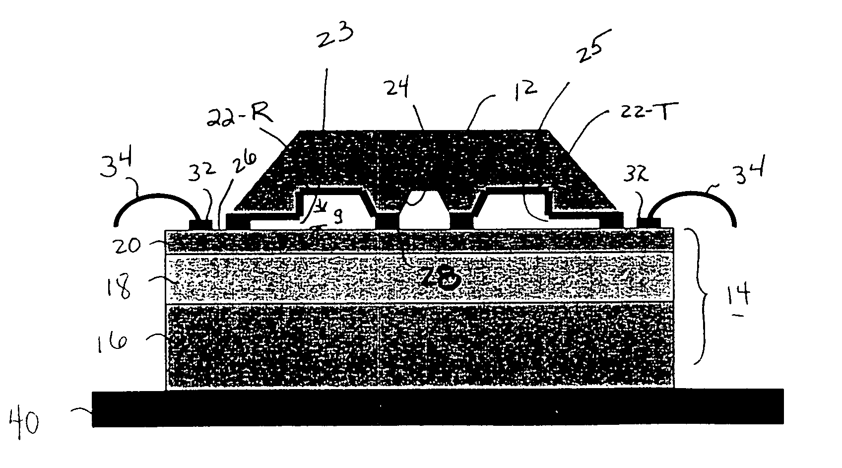
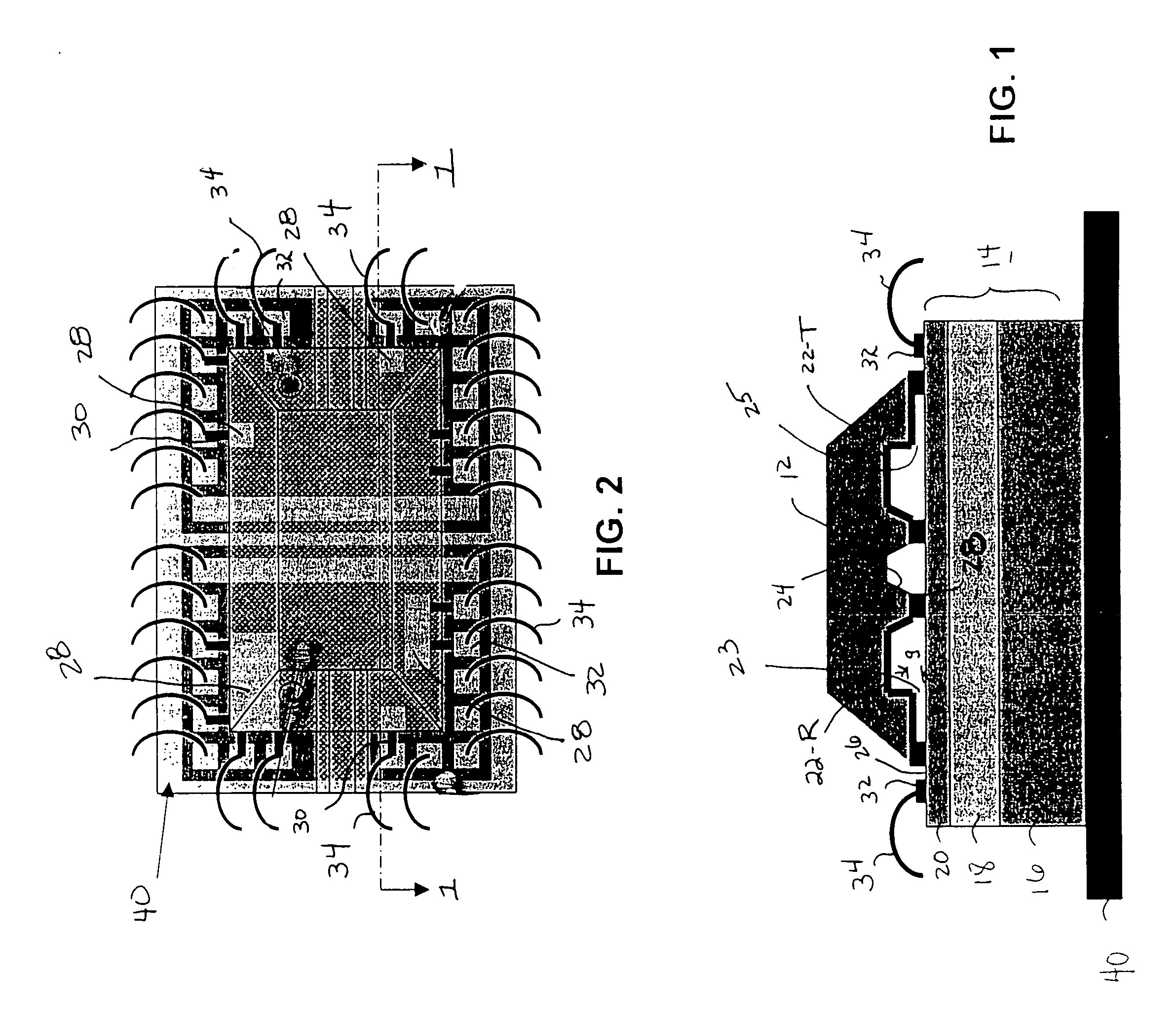
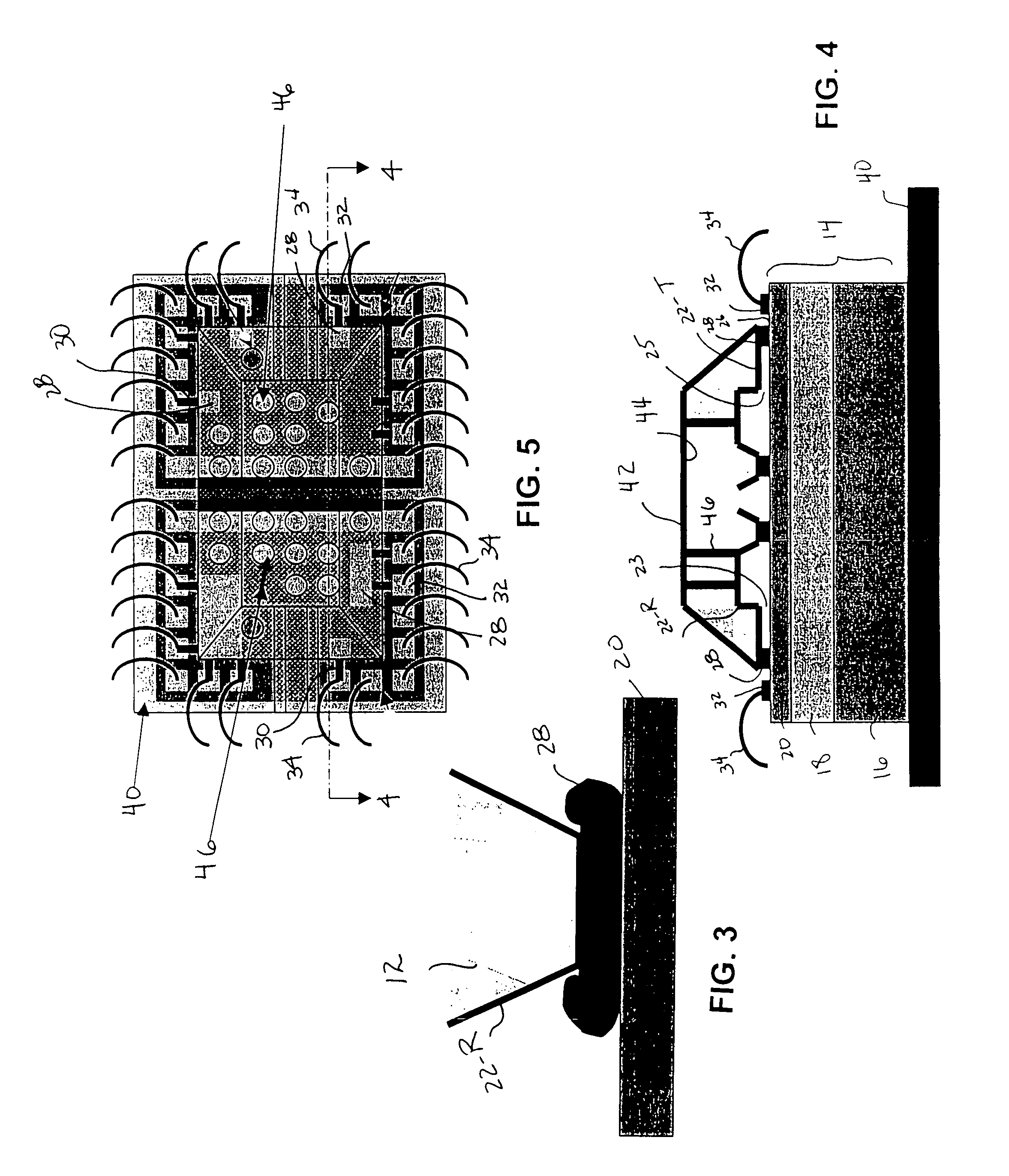
[0025] In order to simultaneously achieve an EMI / EMC shield and optical coupling for a silicon-based opto-electronic integrated circuit formed within an SOI structure, a very low electrical impedance arrangement at electro-magnetic frequencies is required. The interface for the optical coupling also needs to be tightly controlled in order to provide the requisite evanescent coupling between a free space optical beam coupler and the SOI structure. As discussed above, the EMI / EMC shield needs to be such that, for example, an electronic transmitter circuit is significantly electro-magnetically isolated from electronic receiver circuitry (and vice versa). Additionally, the structure needs to electro-magnetically isolate the opto-electronic circuits from external, unwanted EMI radiation sources. It is to be noted that the structural requirements for EMI shielding and EMC shielding are essentially equivalent and will be treated as such for the purposes of the present invention. The EMC sh...


PUM


Abstract

An SOI-based opto-electronic structure includes various electronic components disposed with their associated optical components within a single SOI layer, forming a monolithic arrangement. EMI/EMC shielding is provided by forming a metallized outer layer on the surface of an external prism coupler that interfaces with the SOI layer, the metallized layer including transparent apertures to allow an optical signal to be coupled into and out of the SOI layer. The opposing surface of the prism coupler may also be coated with a metallic material to provide additional shielding. Further, metallic shielding plates may be formed on the SOI structure itself, overlying the locations of EMI-sensitive electronics. All of these metallic layers are ultimately coupled to an external ground plane to isolate the structure and provide the necessary shielding.

Description

CROSS-REFERENCE TO RELATED APPLICATION [0001] The present application claims the benefit of Provisional Application No. 60 / 530,520, filed Dec. 18, 2003.TECHNICAL FIELD [0002] The present invention relates to EMI-EMC shielding for opto-electronic circuits and, more particularly, to the provision of a shielding arrangement for a silicon-based opto-electronic circuits formed within a silicon-on-insulator (SOI) structure. BACKGROUND OF THE INVENTION [0003] Optical transmitters and receivers are widely used in various communication applications, such as for Local Area Networks (LANs). An optical transmitter typically produces either analog or digital optical signals based upon input electrical signals. Similarly, an optical receiver receives optical input signals and produces electrical output signals. For many applications, two-way communications are desirable. Accordingly, an optical transmitter and receiver may be paired within a housing and thus be defined as an “optical transceiver ...

Claims


Application Information

Patent Timeline
Patent Type & Authority Applications(United States)
IPC IPC(8): G02B6/42
CPCG02B6/42G02B6/4277G02B6/4246H01L2224/48091H01L2224/49175H01L2924/00014
Inventor PIEDE, DAVIDGHIRON, MARGARETGOTHOSKAR, PRAKASHMONTGOMERY, ROBERT KEITHPATEL, VIPULKUMARSHASTRI, KALPENDUPATHAK, SOHAMYANUSHEFSKI, KATHERINE A.
Owner CISCO TECH INC
Why Eureka
Try Eureka