

Method and apparatus for co-verification of digital designs
a digital system and co-verification technology, applied in error detection/correction, instruments, cad circuit design, etc., can solve the problems of not allowing flip-flop clocking and very slow simulation
- Summary
- Abstract
- Description
- Claims
- Application Information
AI Technical Summary
Benefits of technology
Problems solved by technology
Method used
Image

Examples
Embodiment Construction
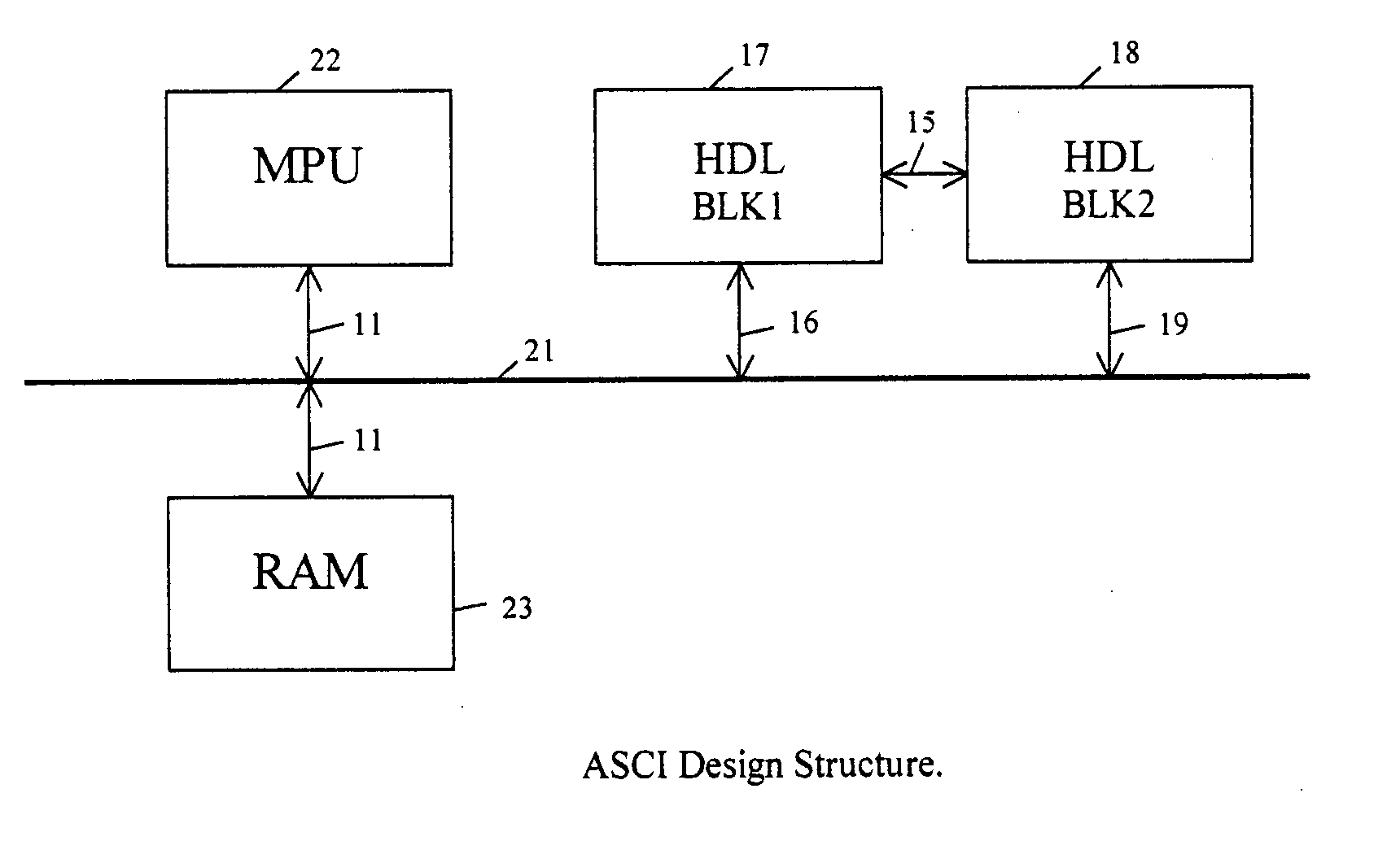
[0017] A typical ASIC or large FPGA system design 7 comprised of microprocessor unit (MPU) 22, random access memory (RAM) 23 and hardware logic blocks, such as blocks 17 and 18 is illustrated in the block diagram of FIG. 1. Microprocessor 22 executes a program residing in RAM 23 and provides processing data on local bus 11. Processor 22 spends most of its time processing-instructions provided by RAM 23. However, when needed, MPU 22 communicates also with HDL blocks 17 and 18. This kind of asynchronous communication of microprocessor 22 with hardware logic blocks 17 or 18 is called a transactional interface, and it is started either by processor 22 attempting to read or write into hardware logic blocks 17 or 18, or by an interrupt generated by one of hardware logic blocks 17 or 18 and sent over bus 11. Hardware logic block 17 is connected to bus 11 via bus 16 that may be a subset of bus 11. Similarly, hardware logic block 18 is connected to bus 11 via local bus 19 that may be a diffe...
PUM
 Abstract
Description
Claims
Application Information