
Semiconductor light-emitting device and method of manufacturing the same

a technology of semiconductors and light-emitting devices, which is applied in the direction of semiconductor lasers, solid-state devices, lasers, etc., can solve the problems of increasing the amount of oscillation, increasing the current confinement by the ridge of the related art, and reducing the reliability of the device, so as to improve the device characteristics

Inactive Publication Date: 2005-06-30
SONY CORP
View PDF3 Cites 25 Cited by
  • Summary
  • Abstract
  • Description
  • Claims
  • Application Information

AI Technical Summary

Benefits of technology

[0010] In view of the foregoing, it is an object of the invention to provide a semiconductor light-emitting device capable of improving the device characteristics such as life and reliability by use of the current confinement layer formed by oxidation, and a method of manufacturing the same.
[0013] According to the semiconductor light-emitting device or the method of manufacturing the semiconductor light-emitting device of the invention, the oxidized region in the current confinement layer is formed at an optimal temperature from 240° C. to less than 375° C. Therefore, the device life is improved, thereby improving the device characteristics and reliability.

Problems solved by technology

However, the current confinement by the ridge of the related art has a several problems as mentioned below.
The absorption loss of the light or the distortion of the active layer increases the amount of oscillation current and largely decreases reliability of the device.
This results in an increase in operation voltage, thereby power consumption is increased.
The increased power consumption largely affects on the device life and this will be a serious problem for a practical application.
However, the volume of the current confinement layer formed by oxidation shrinks and generates distortion in the semiconductor layers including the active layer formed above and below the current confinement layer.
The distortion adversely affects on the device characteristics and reliability, in particular, the device life is significantly deteriorates.

Method used


Image

  • Semiconductor light-emitting device and method of manufacturing the same
  • Semiconductor light-emitting device and method of manufacturing the same
  • Semiconductor light-emitting device and method of manufacturing the same

Examples


example 1

[0064] Similar to the above embodiment, a laser diode was fabricated. The oxidation temperature for forming the oxidized region 18B was 360° C. Accelerated aging test was conducted on the obtained laser diode. The current was not passed from the start (0 h) to 0.5 h after and the temperature was kept at 25° C. The current was not passed from 0.5 h after the start to 2.5 h after and the temperature was raised from 25° C. to 70° C. The current was passed 2.5 h after the start at 70° C. The results are shown in FIG. 8.

examples 2 to 4

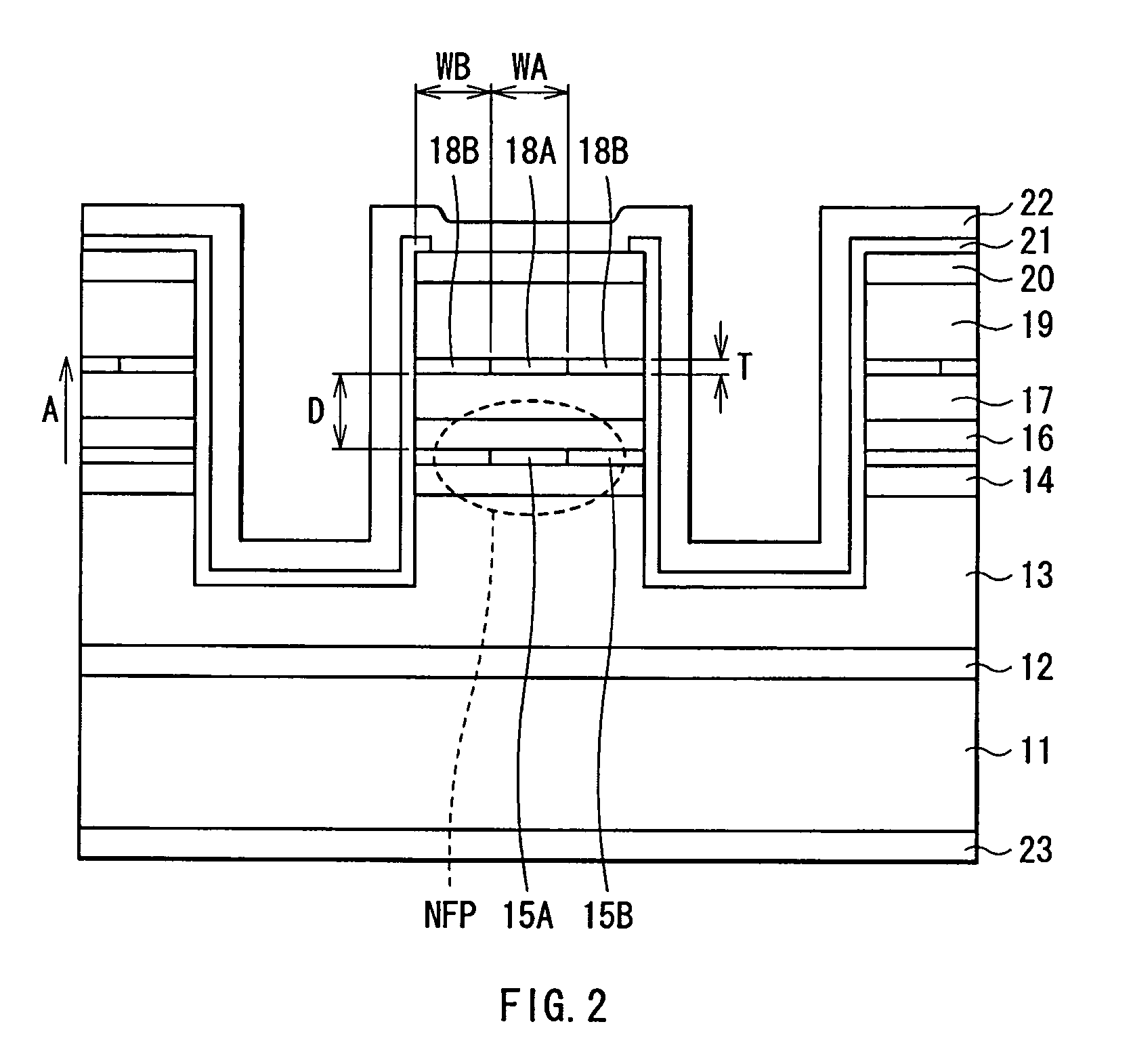
[0067] Like the embodiment, laser diodes were fabricated. The distance D between the active layer 15 and the current confinement layer 18 was 120 nm in Example 2, 210 nm in Example 3 and 220 nm in Example 4. Absorption coefficient was examined on the laser diodes of Example 2 to 4. The results are shown in FIG. 9 together with a curve representing the correlation relation of distance D and the absorption coefficient on the basis of the results of Examples 2 to 4. The absorption coefficient in the laser diode using the current confinement by conventional ridge is 8 cm−1 or less. This is also shown in FIG. 9.

[0068] As can be seen from FIG. 9, the absorption coefficients of Example 3 having the distance D between the active layer 15 and the current confinement layer 18 of 210 nm and Example 4 having the distance D of 220 nm were lower compared to that of the conventional structure. On the other hand, the absorption coefficient of Example 2 having the distance D of 120 nm was higher th...


PUM


Abstract

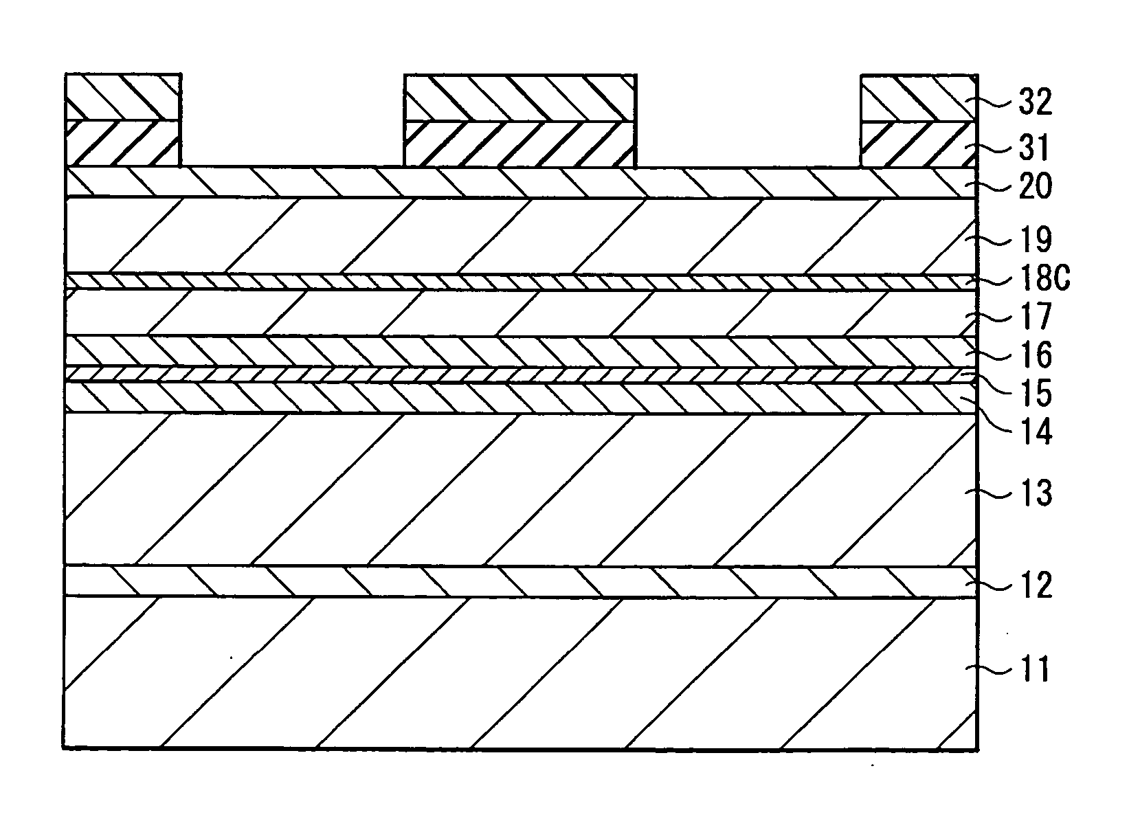
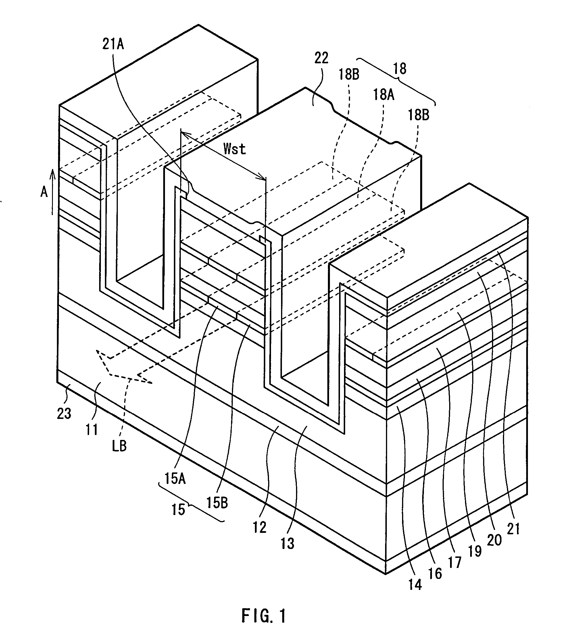
A semiconductor light-emitting device capable of improving device characteristics such as life and reliability is provided. A current confinement layer includes a non-oxidized region made of AlAs or the like corresponding to a current injection region in an active layer, and an oxidized region made of aluminum oxide corresponding to a non-current injection region. The oxidized region is formed by forming a non-oxidized layer made of AlAs or the like and then oxidizing part of the non-oxidized layer at a temperature from 240° C. to less than 375° C. The thickness of the oxidized region is preferably from 10 nm to 1000 nm. The width of the one side of the oxidized region is one time or more of the width of the non-oxidized region or seven times or less thereof The distance between current confinement layer and the active layer is preferably 50 nm or more, or 500 nm or less, and more preferably 180 nm or more.

Description

BACKGROUND OF THE INVENTION [0001] 1. Field of the Invention [0002] The present invention relates to a semiconductor light-emitting device including a current confinement layer formed by oxidation and a method of manufacturing the same, and particularly to a semiconductor light-emitting device suitable for a red laser having a wavelength of about 600 nm to 700 nm and a method of manufacturing thereof. [0003] 2. Description of the Related Art [0004] A laser diode using AlGaInP as a base material can obtain red emission having a wavelength of 600 nm to 700 nm and is widely used as a light source for a high-density recording by DVD (Digital Versatile Disc) or the like. [0005] The red laser using AlGaInP is generally formed with a strip-shaped ridge by removing part of a p-type semiconductor layer by etching for current confinement. Upon directly forming an electrode on the ridge, leakage current is generated. Therefore, in order to prevent the leakage current, a buried layer including ...

Claims


Application Information

Patent Timeline
Patent Type & Authority Applications(United States)
IPC IPC(8): H01S5/343H01L29/24H01L29/26H01S5/183H01S5/22
CPCB82Y20/00H01L33/145H01S5/0021H01S5/22H01S2301/18H01S5/2231H01S5/34326H01S2301/14H01S5/2215
Inventor HINO, TOMONORINARUI, HIRONOBUKAWASUMI, TAKAYUKINAGATAKE, TSUYOSHIKUROMIZU, YUICHIKAWASAKI, TADAHIKOKOBAYASHI, NORIKOSHIOZAKI, MASAKIMITOMO, JUGOKOMINE, MICHIKO
Owner SONY CORP
Learn More