Poly crystalline silicon semiconductor device and method of fabricating the same

a technology of polycrystalline silicon and semiconductors, applied in the field of polycrystalline silicon semiconductor devices, can solve the problems of easy damage to plastics, unnecessary parasitic capacitance generation, distortion and delay of gate signal transfer, etc., and achieve the effect of eliminating the cause and preventing distortion and delay of gate signal

Active Publication Date: 2005-06-30
SAMSUNG ELECTRONICS CO LTD
View PDF3 Cites 17 Cited by
  • Summary
  • Abstract
  • Description
  • Claims
  • Application Information

AI Technical Summary

Benefits of technology

[0012] The present invention provides a poly crystalline silicon semiconductor device and a method of fabricating the same to efficiently prevent the distortion and delay of gate signals caused from a pa

Problems solved by technology

However, the defect of plastic being easily damaged by heat requires a low temperature process to apply a plastic substrate to an LCD.
However, the method provided by Carry et al. results in a silicon film remaining, as an active region, under gates and as an unnecessary capacitive element under gate bus lines.
The silicon remaining under the gate bus lines and having a high dielectric constant gen

Method used


Image

  • Poly crystalline silicon semiconductor device and method of fabricating the same
  • Poly crystalline silicon semiconductor device and method of fabricating the same
  • Poly crystalline silicon semiconductor device and method of fabricating the same

Examples


Embodiment Construction

[0032] The present invention will now be described more fully with reference to the accompanying drawings, in which an exemplary embodiment of the invention is shown.

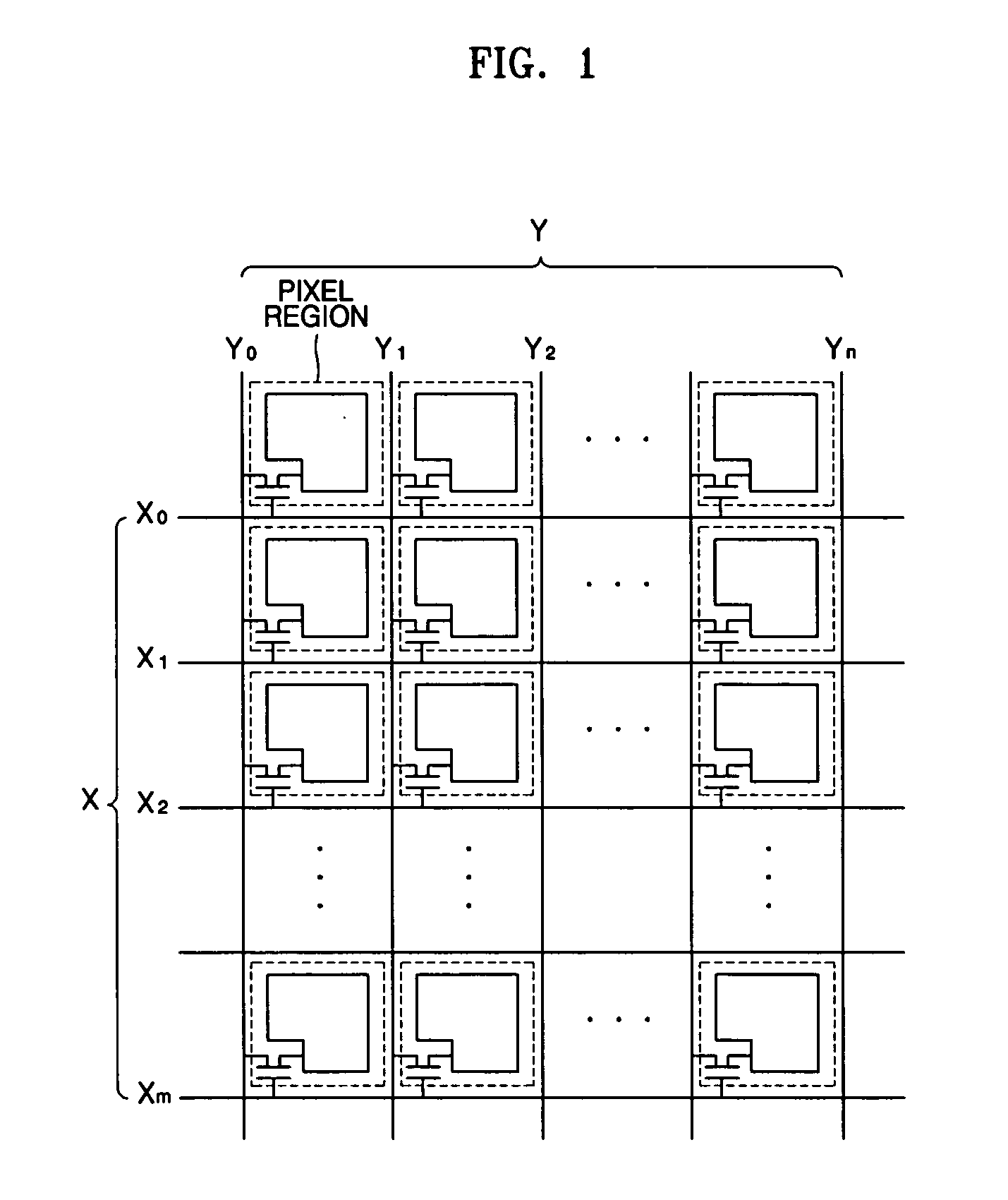
[0033] A thin film transistor (TFT) according to the present invention is arranged on a substrate in an X-Y matrix type and applied to an active matrix liquid crystal display (AM-LCD) or an active matrix organic light emitting device (AM-OLED). An X-Y matrix structure is formed of a plurality of gate bus lines X0 through Xm and a plurality of source bus lines Y0 through Yn that are perpendicular to each other as shown in FIG. 1. In addition, TFTs and pixel electrodes are arranged in pixel regions, which are defined in the crossing portions of the bus lines. Here, the pixel electrodes may be the pixel electrodes of an OLED and the pixel electrodes of an LCD.

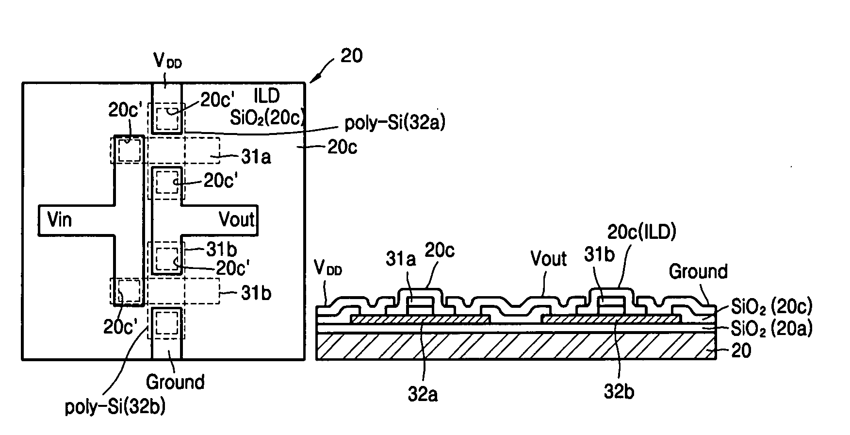
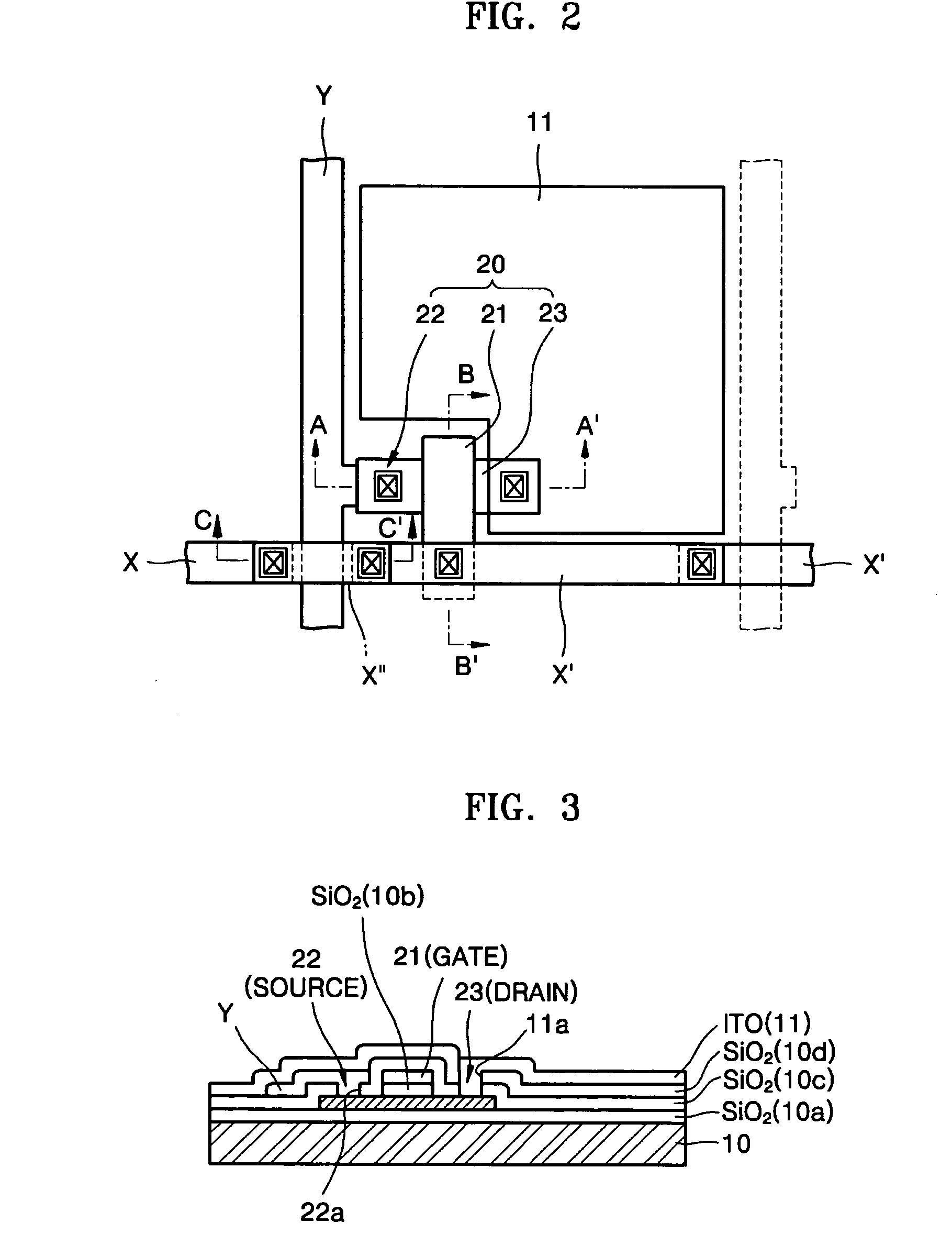
[0034]FIG. 2 is a plain view illustrating one pixel region of the TFT of FIG. 1. Here, the pixel region of FIG. 2 illustrates the arrangement of a TFT 20, a pixel e...


PUM


Abstract

Provided are a poly crystalline silicon semiconductor device and a method of fabricating the same. Portions of a silicon layer except for gates are removed to reduce a parasitic capacitance caused from the silicon layer existing on gate bus lines. The silicon layer exists under the gates only, thus the parasitic capacitance is reduced and the deterioration and the delay of signals are prevented. Accordingly, the poly crystalline silicon semiconductor device, such as a thin film transistor, has excellent electric characteristics.

Description

BACKGROUND OF THE INVENTION [0001] Priority is claimed to Korean Patent Applications No. 10-2003-0100618, filed on Dec. 30, 2003, and No. 10-2004-0052982, filed on Jul. 8, 2004, in the Korean Intellectual Property Office, the disclosure of which is incorporated herein in its entirety by reference. [0002] 1. Field of the Invention [0003] The present invention relates to a poly crystalline silicon semiconductor device and a method of fabricating the same, and more particularly, to a poly crystalline silicon thin film transistor (TFT) and a method of fabricating the same for efficiently reducing the capacitance of gate bus lines. [0004] 2. Description of the Related Art [0005] Poly crystalline silicon, which will be referred to as poly-Si hereafter, has characteristics of high mobility and excellent optical stability compared to amorphous silicon. Such poly-Si is used in various application fields, mainly in TFT and memory devices. Poly-Si TFTs are used as switching devices in displays...

Claims


Application Information

Patent Timeline
IPC IPC(8): H01L29/786H01L21/20H01L21/336H01L21/77H01L21/84H01L27/12H01L29/423
CPCH01L27/124H01L29/42384
Inventor KIM, DO-YOUNGNOGUCHI, TAKASHI
Owner SAMSUNG ELECTRONICS CO LTD
Why Eureka
Try Eureka