

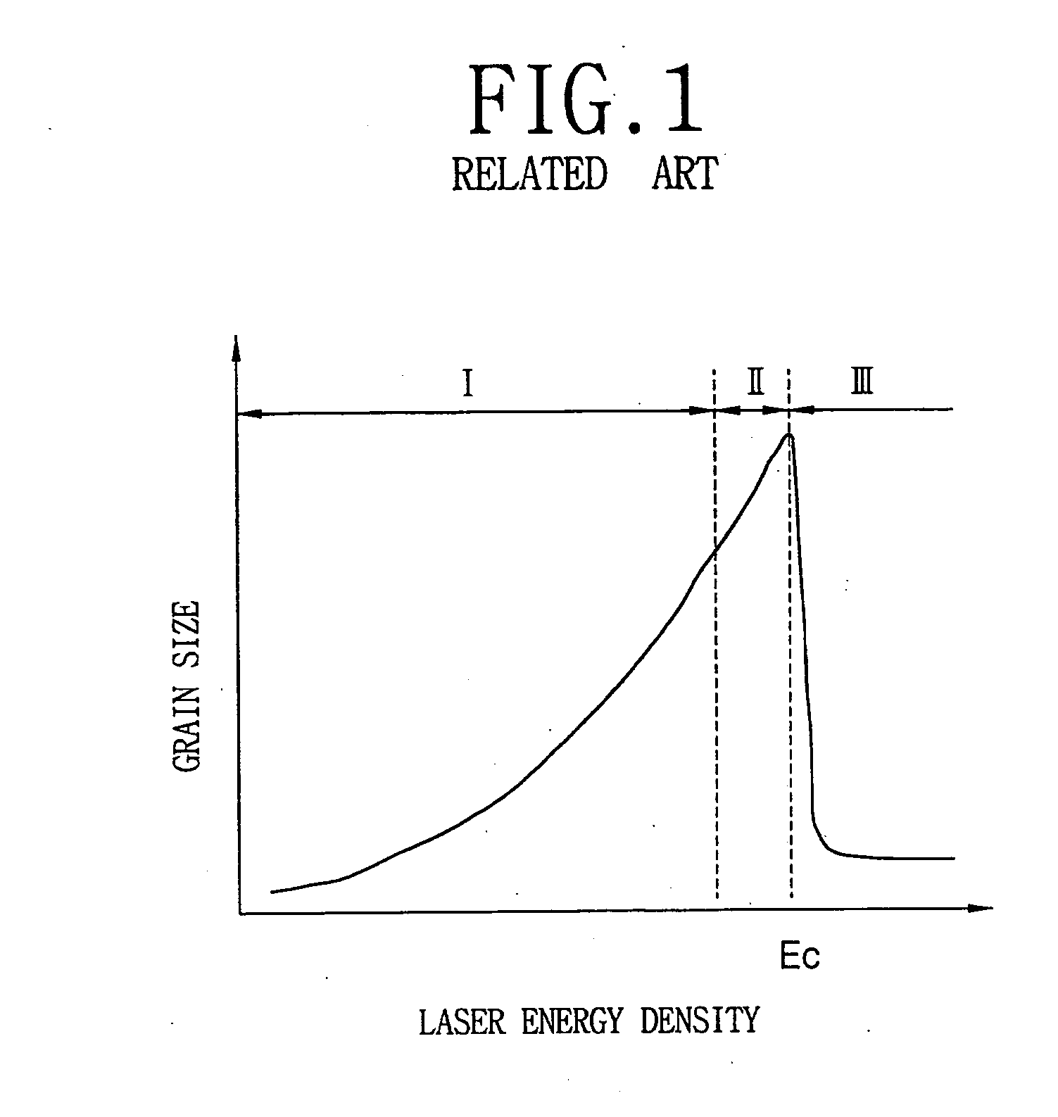
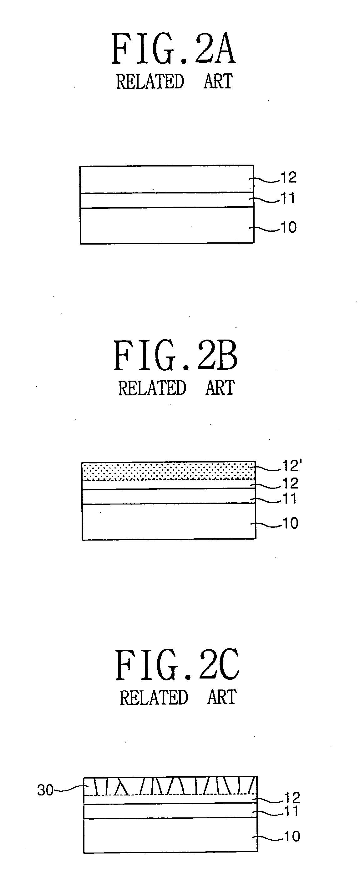
Laser mask and crystallization method using the same
a crystallization method and laser mask technology, applied in the field of laser mask and crystallization method using the same, can solve the problems of reduced signal distortion, increased picture quality, and use in peripheral circuits, and achieve the effect of improving crystallization characteristics and improving crystallization characteristics
- Summary
- Abstract
- Description
- Claims
- Application Information
AI Technical Summary
Benefits of technology
Problems solved by technology
Method used
Image

Examples
Embodiment Construction
[0058] Reference will now be made in detail to the embodiments of the present invention, examples of which are illustrated in the accompanying drawings.
[0059]FIG. 6A is a plan view illustrating an example of a laser mask used for a sequential lateral solidification (SLS), which is designed to shorten crystallization time compared to the related art. Referring to FIG. 6A, a laser mask 270 includes a slit type pattern 275 having a rectangular transmitting region 273 with a predetermined width and length. The laser mask 270 includes two rectangular transmitting regions 273 for transmitting light and blocking region 274 for blocking light. A laser beam transmitted through the transmitting regions 273 of the slit 275 crystallizes a silicon thin film according to the shape (e.g., rectangular shape) of the transmitting regions 273.
[0060] Referring to FIG. 6B, however, an edge portion (E) of the crystallized silicon thin film has a round shape different from the mask pattern (the slit 275...
PUM
| Property | Measurement | Unit |
|---|---|---|
| driving voltage | aaaaa | aaaaa |
| driving voltage | aaaaa | aaaaa |
| melting point | aaaaa | aaaaa |
Abstract
Description
Claims
Application Information