
Organic electroluminescent display device and method of fabricating the same

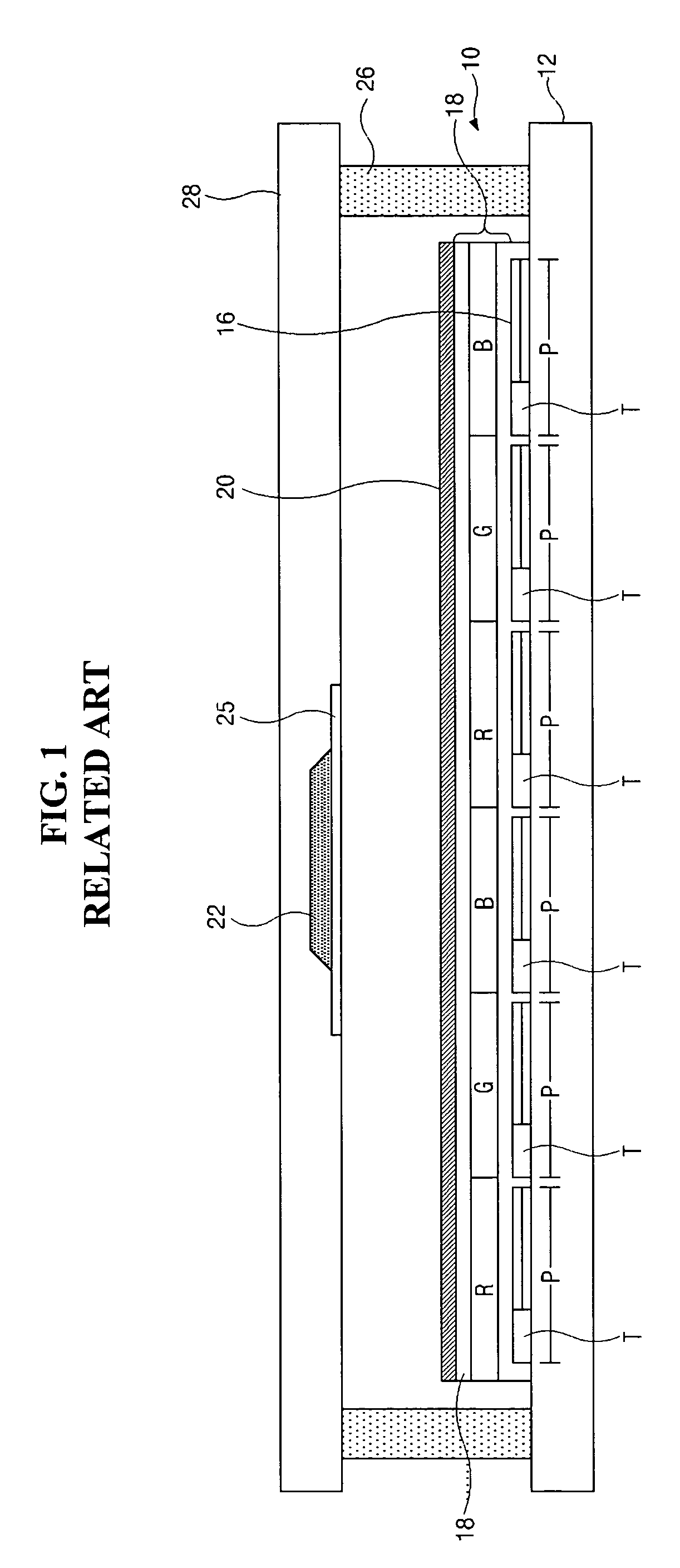
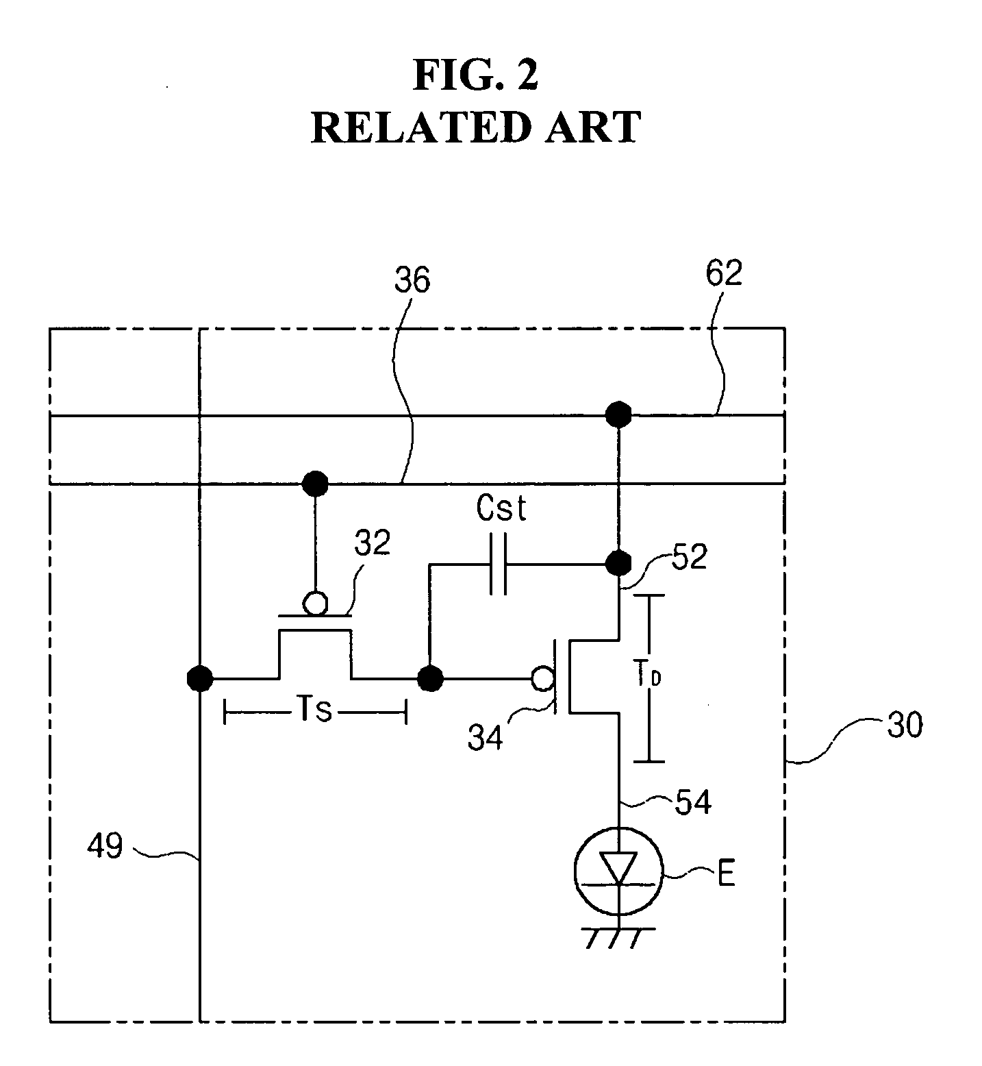
a technology electroluminescent display device, which is applied in the direction of instruments, discharge tube luminescnet screens, static indicating devices, etc., can solve the problems of high low power consumption of electroluminescent display device, and preventing use of large-area displays, etc., to achieve high aperture ratio, improve yield and productivity, and high brightness

Active Publication Date: 2005-06-30
LG DISPLAY CO LTD
View PDF15 Cites 42 Cited by
  • Summary
  • Abstract
  • Description
  • Claims
  • Application Information

AI Technical Summary

Benefits of technology

[0021] An object of the present invention is to provide an organic electroluminescent display device and a method of fabricating the same having a high aperture ratio and displaying high definition images.
[0022] Another object of the present invention is to provide an organic electroluminescent display device and a method of fabricating the same having an improved yield and productivity.
[0023] Another object of the present invention is to provide an organic electroluminescent display device and a method of fabricating the same that are reliable.

Problems solved by technology

The organic electroluminescent display device also has a low power consumption, high brightness, and a short response time.
However, the passive matrix-type organic electroluminescent display devices have a high power consumption, thereby preventing use in large area displays.
Thus, even if the array elements are properly well formed, if the organic light-emitting layer to be formed to a thickness of about 1,000 Å is improperly formed due to impurities or other factors, the resulting OELD device is rejected as bad.
Accordingly, the yield of the OELD device is reduced because of the impurities and other factors in the organic light-emitting forming processes, thereby resulting in a loss of manufacturing costs and source materials for the thin film transistor.
However, the bottom emission mode OELD device has a reduced aperture ratio.
Thus, the bottom emission mode OELD device is not suited for a high aperture device.
Additionally, the top emission mode OELD device has a long lifetime.
However, in the top emission mode OELD device, since a cathode electrode is generally disposed over the organic light-emitting layer, a choice of material with which to make the cathode electrode is limited.
Accordingly, the transmittance of light is limited, and a light-emitting efficacy is reduced.

Method used


Image

  • Organic electroluminescent display device and method of fabricating the same
  • Organic electroluminescent display device and method of fabricating the same
  • Organic electroluminescent display device and method of fabricating the same

Examples


first embodiment

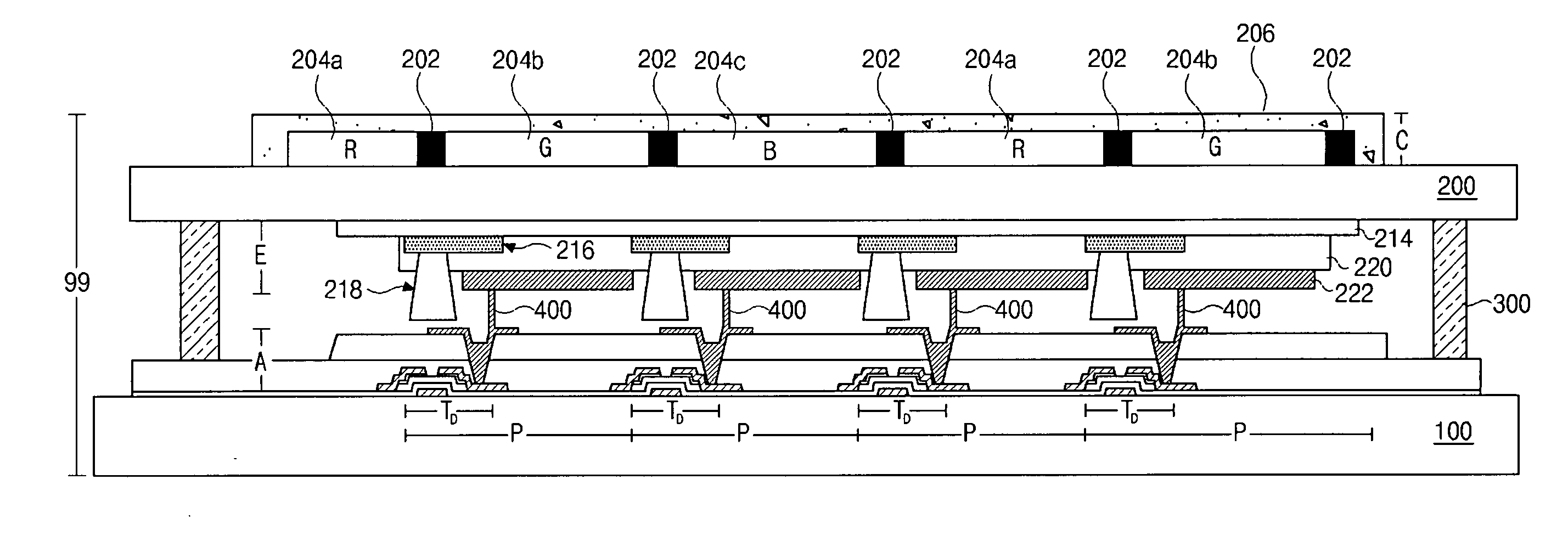
[0041] As shown in FIG. 3, the OELD device 99 of the first embodiment includes a first substrate 100 and a second substrate 200 that are spaced apart from and face each other. A sealant 300 is formed between the first and second substrates 100 and 200 to bond the first and second substrates 100 and 200 together. An array part A including a plurality of thin film transistors TD is formed on an inner surface of the first substrate 100. An emission part E is formed on an inner surface of the second substrate 200 (i.e., a surface facing the first substrate 100), and a color part C is formed on an outer surface of the second substrate 200 (i.e., a surface opposite to the inner surface of the second substrate 200).

[0042] In FIG. 3, the thin film transistor TD functions as a driving element of the OELD device. Although not shown, a switching element, a gate line, a data line, and a power line are typically formed on the inner surface of the first substrate 100. The switching element (not s...

second embodiment

[0064] As shown in FIG. 6, the OELD device 99 of the second embodiment may include a first substrate 100 and a second substrate 200 that are spaced apart from and face each other. A sealant 300 is formed between the first and second substrates 100 and 200 to bond the first and second substrates 100 and 200 together. An array part A including a plurality of thin film transistors TD is formed on an inner surface of the first substrate 100. An emission part E is formed on an inner surface of the second substrate 200 (i.e., a surface facing the first substrate 100), and a color displaying element is formed on an outer surface of the second substrate 200 (i.e., a surface opposite to the inner surface of the second substrate 200).

[0065] In FIG. 6, the thin film transistor TD functions as a driving element of the OELD device. Although not shown, a switching element, a gate line, a data line, and a power line are typically formed on the inner surface of the first substrate 100. The switchin...

third embodiment

[0074] As shown in FIG. 7, the OELD device of the third embodiment includes a first substrate 100 having an array part that includes a plurality of thin film transistors TD thereon, a second substrate 200 having an emission part on a surface facing the first substrate 100, and a third substrate 300 having a color displaying element.

[0075] A sealant 310 is formed between the first and second substrates 100 and 200 to bond the first and second substrates 100 and 200 together. The third substrate 300 including coloring elements 304a, 304b and 304c is attached to an outer surface of the second substrate 200 using an adhesion layer 308, which is formed on an entire surface of the third substrate 300.

[0076] In FIG. 7, the thin film transistor TD functions as a driving element of the OELD device. Although not shown, a switching element, a gate line, a data line, and a power line are also typically formed on the inner surface of the first substrate 100. The switching element (not shown) an...


PUM

PropertyMeasurementUnit
Coloraaaaaaaaaa
Adhesion strengthaaaaaaaaaa
Transparencyaaaaaaaaaa

Abstract

An organic electroluminescent display device includes first and second substrates facing and spaced apart from each other, gate and data lines on an inner surface of the first substrate and crossing each other to define a pixel region, a switching element at a crossing point of the gate and data lines, a driving element connected to the switching element, a first electrode on an inner surface of the second substrate, an organic light-emitting layer on the first electrode in the pixel region, a second electrode on the organic light-emitting layer in the pixel region and electrically connected to the driving element, and a coloring element on an outer surface of the second substrate in the pixel region.

Description

[0001] The present invention claims the benefit of Korean Patent Application No. 2003-0100603 filed in Korea on Dec. 30, 2003, which is hereby incorporated by reference. BACKGROUND OF THE INVENTION [0002] 1. Field of the Invention [0003] The present invention relates to an electroluminescent display device, and more particularly, to an organic electroluminescent display device and a method of fabricating the same. [0004] 2. Discussion of the Related Art [0005] In general, an organic electroluminescent display device emits light by injecting electrons from a cathode electrode and holes from an anode electrode into an emissive layer, combining the electrons and the holes to generate an exciton, and by transiting the exciton from an excited state to a ground state. Since the organic electroluminescent display device does not require an additional light source due to its self-luminescence property, the organic electroluminescent display device has a small size and is light weight, as co...

Claims


Application Information

Patent Timeline
IPC IPC(8): H05B33/22G09G3/30G09G3/32H01L27/32H01L51/52H01L51/56H05B33/00H05B33/02H05B33/04H05B33/06H05B33/10H05B33/12H05B33/26H05B44/00
CPCG09G3/3208H01L27/322H01L27/3246H01L27/3251Y10S428/917H01L51/5284H01L51/56H01L2251/5315H01L51/5253H10K59/127H10K59/38H10K59/122H10K2102/3026H10K71/00H10K59/8792H10K59/873H05B33/22H10K50/844H10K50/865
Inventor PARK, JAO-YONGLEE, NAM-YANG
Owner LG DISPLAY CO LTD
Features
  • Generate Ideas
  • Intellectual Property
  • Life Sciences
  • Materials
  • Tech Scout
  • Unparalleled Data Quality
  • Higher Quality Content
  • 60% Fewer Hallucinations
Learn More