Dual panel type organic electroluminescent display device and method of fabricating the same

a technology substrate, which is applied in the direction of discharge tube luminescnet screens, identification means, instruments, etc., can solve the problems of low direct current voltage of organic electroluminescent display devices, waste of all manufacturing costs and source materials required for array elements, and failure of oeld devices, etc., to achieve high aperture ratio, improve yield and productivity, and high definition

Inactive Publication Date: 2005-06-30
LG DISPLAY CO LTD
View PDF11 Cites 48 Cited by
  • Summary
  • Abstract
  • Description
  • Claims
  • Application Information

AI Technical Summary

Benefits of technology

[0021] An object of the present invention is to provide a dual panel type organic electroluminescent display device and a method of fabricating the same having a high aperture ratio and high definition images.
[0022] Another object of the present invention is to provide a dual panel type orga

Problems solved by technology

In addition, the organic electroluminescent display device is driven by a low direct current voltage and a short response time.
Because all elements of the organic electroluminescent display device are solid, the organic electroluminescent display device can be used in a wide range of temperatures and is unlikely to be damaged by external impacts.
Thus, even if the array elements are properly manufactured, if the organic light-emitting layer to be formed to a thickness of about 1,000 Å is improperly manufactured due to impurities or other factors, the resulting OELD device will be rejected as bad

Method used


Image

  • Dual panel type organic electroluminescent display device and method of fabricating the same
  • Dual panel type organic electroluminescent display device and method of fabricating the same
  • Dual panel type organic electroluminescent display device and method of fabricating the same

Examples


first embodiment

[0054]FIG. 3 is a cross-sectional view of a dual panel type organic electroluminescent display (OELD) device according to the present invention. In FIG. 3, the dual panel type organic electroluminescent display (OELD) device includes a first substrate 110 and a second substrate 130 that are spaced apart and face each other. An array element layer A including a plurality of thin film transistors T is formed on an inner surface of the first substrate 110. A plurality of connection patterns 120 having a predetermined thickness are formed on the array element layer A. Each connection pattern 120 is connected to each thin film transistor T.

[0055] The predetermined thickness of the connection patterns 120 may be selected from a thickness range such that a pixel driving part and an emission part formed on different substrates are electrically connected to each other by the connection patterns 120. Thus, the thickness of the connection patterns 120 corresponds to a cell gap between the subs...

second embodiment

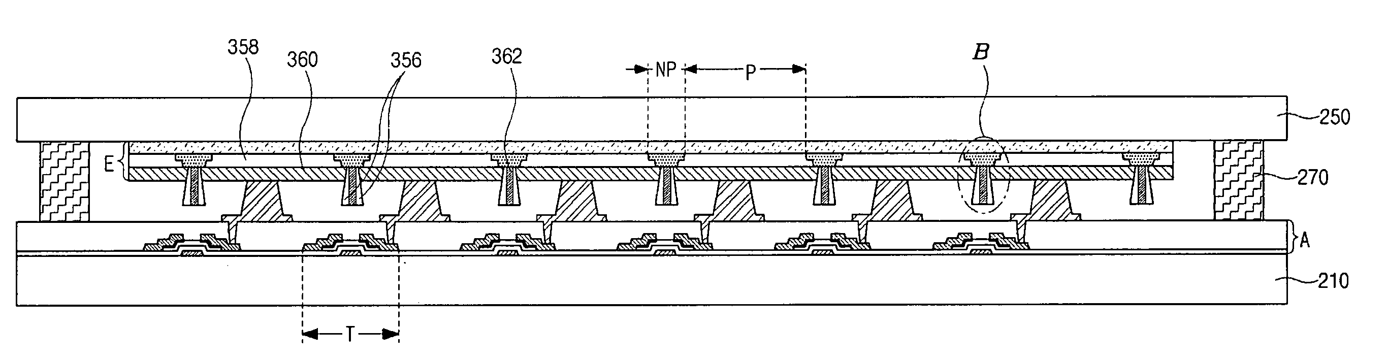
[0071]FIG. 5 is a schematic plan view of a substrate for the dual panel type OELD device according to the present invention, and shows the second substrate including the moisture absorption layer.

[0072] In FIG. 5, a plurality of pixel areas P, each of which is a minimum unit for an image, is defined on a substrate 250 and spaced apart from each other. A space between the pixel areas P is referred to as a non-pixel area NP. A moisture absorption layer 262 is formed corresponding to the non-pixel area NP.

[0073] An insulating pattern 254 and a partition wall 256 of FIG. 4 are sequentially formed under the moisture absorption layer 262. In fact, the moisture absorption layer 262 is separated from a second electrode 260 formed in the pixel area P due to a thickness of the partition wall 256.

[0074]FIGS. 6A to 6C show a dual panel type OELD device according to a third embodiment of the present invention. FIG. 6A is a cross-sectional view of the dual panel type OELD device, FIG. 6B is a v...

fifth embodiment

[0105]FIG. 10 is a cross-sectional view of a dual panel type OELD device according to the present invention. The dual panel type OELD device includes a color filter layer as the full color element.

[0106] As shown in FIG. 10, a first substrate 510 and a second substrate 550 are spaced apart from and facing each other. A color filter layer 552 and a black matrix 554 are formed on an inner surface of the second substrate 550. The color filter layer 552 includes red, green and blue sub-color filters 552a, 552b and 552c, and the black matrix 554 is disposed between adjacent sub-color filters 552a, 552b and 552c of the color filter layer 552. An overcoat layer 558 and a barrier layer 560 are sequentially formed on the color filter layer 552 and the black matrix 554. The overcoat layer 558 planarizes a surface of the second substrate 550 including the color filter layer 552 and the black matrix 554. The barrier layer 560 prevents outgassing from the color filter layer 552.

[0107] A first e...


PUM


Abstract

A dual panel type organic electroluminescent display device includes first and second substrates facing and spaced apart from each other, an array element layer on an inner surface of the first substrate and including a thin film transistor, a connection pattern on the array element layer and electrically connected to the thin film transistor, a first electrode on an inner surface of the second substrate, a partition wall on the first electrode in a non-pixel area between adjacent pixel areas, an organic light-emitting layer on the first electrode in the pixel area, a second electrode on the organic light-emitting layer in the pixel area and electrically connected to the connection pattern, a moisture absorption layer on the partition wall, and a seal pattern between the first and second substrates along a peripheral portion.

Description

[0001] The present invention claims the benefit of Korean Patent Application Nos. P2003-0099919 filed on Dec. 30, 2003, P2003-0099937 filed on Dec. 30, 2003, and P2003-0101281 filed on Dec. 31, 2003, all of which are hereby incorporated by reference. BACKGROUND OF THE INVENTION [0002] 1. Field of the Invention [0003] The present invention relates to an organic electroluminescent display device and method of fabricating the same, and more particularly, to a dual panel type organic electroluminescent display device and a method of fabricating the same. [0004] 2. Discussion of the Related Art [0005] Among flat panel display devices, since an organic electroluminescent display device is self-luminescent and does not require an additional light source, the organic electroluminescent display device has a wide viewing angle, high contrast ratio, and a small size and is light weight, as compared to a liquid crystal display device. The organic electroluminescent display device also has a low...

Claims


Application Information

Patent Timeline
IPC IPC(8): G09F9/00G09F9/30H05B33/04G09F9/33G09F13/22G09G3/32H01L27/15H01L27/32H01L51/50H01L51/52H05B33/00H05B33/02H05B33/06H05B33/10H05B33/12H05B33/14H05B33/22H05B33/28H05B44/00
CPCH01L27/3246H01L2251/5315H01L51/5259H01L27/3251H01L27/1255H10K59/127H10K59/122H10K2102/3026H10K59/874G09G3/3208H01L27/156H10K50/846
Inventor PARK, JAE-YONGKIM, KWAN-SOU
Owner LG DISPLAY CO LTD
Why Eureka
Try Eureka