Switched capacitor circuit compensation apparatus and method

a switched capacitor and circuit compensation technology, applied in the field of switching capacitor circuit compensation apparatus and method, can solve the problems of settling errors, settling errors represent a potentially significant source of non-linear distortion in switched capacitor circuits, and settling errors almost inevitably, so as to achieve advantageous use of wireless communication devices, increase the reference current, and reduce the reference current

Active Publication Date: 2005-06-30
TELEFON AB LM ERICSSON (PUBL)
View PDF4 Cites 38 Cited by
  • Summary
  • Abstract
  • Description
  • Claims
  • Application Information

AI Technical Summary

Benefits of technology

[0007] An exemplary circuit according to the present invention comprises a switched capacitor circuit comprising one or more switched capacitors and an amplifier configured to generate an output current proportional to a reference current, wherein a settling time of the switched capacitor circuit depends on an effective capacitance of the one or more switched capacitors as seen by the output current; and further comprises a compensation circuit configured to increase and decrease the reference current as needed to charge a reference capacitor at a targeted slew rate determined by a clock frequency of the switched capacitor circuit. An exemplary compensation circuit comprises a delay locked loop circuit configured to increase the reference current if a detected slew rate of the compensation circuit is less than the targeted slew rate, and to decrease the reference current if the detected slew rate is greater than the targeted slew rate. The exemplary circuit may be implemented as an Integrated Circuit (IC) device, and may be advantageously used wireless communication devices, such as in filters and analog-to-digital converters used in radio base stations and mobile terminals, for example.

Problems solved by technology

Settling errors arise if the sampling phase ends before the sampling capacitor has fully charged (or discharged) to the level of the signal being sampled, or if the integration phase ends before completion of charge transfer to the integration capacitor.
Such settling errors represent a potentially significant source of non-linear distortion in switched capacitor circuits.
In practice, settling errors arise almost inevitably because switched capacitor circuits vary from their nominal or designed-for parameters.

Method used


Image

  • Switched capacitor circuit compensation apparatus and method
  • Switched capacitor circuit compensation apparatus and method
  • Switched capacitor circuit compensation apparatus and method

Examples


Embodiment Construction

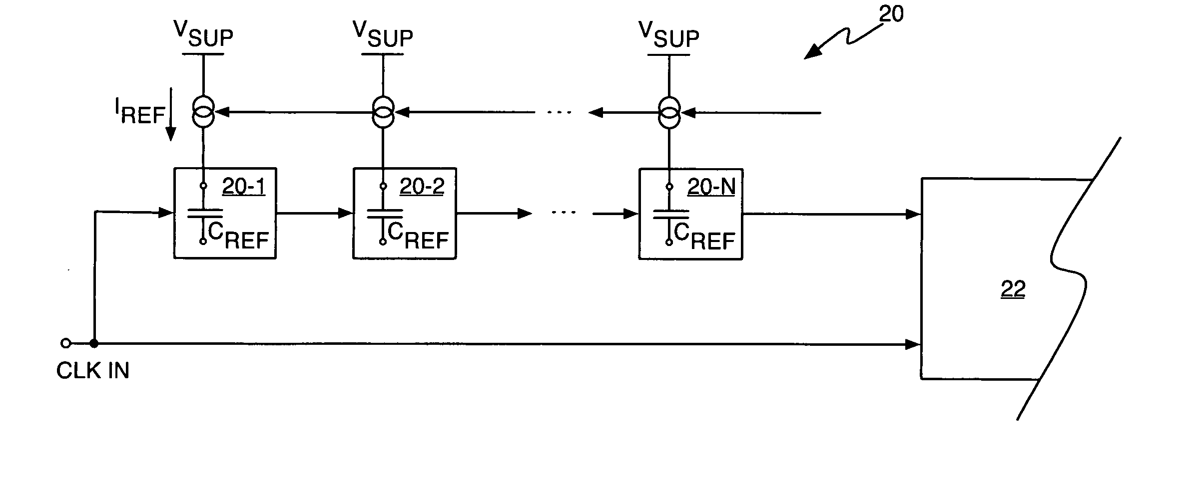
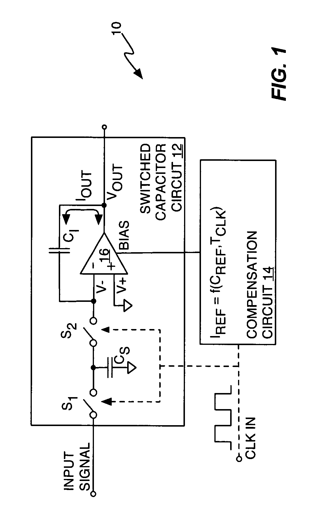
[0015]FIG. 1 illustrates a circuit 10 comprising a switched capacitor circuit 12 and an associated compensation circuit 14. Switched capacitor circuit 12 may be configured as part of an Integrated Circuit (IC) for use in signal filtering or analog-to-digital conversion, for example. As is understood by those skilled in the art, switched capacitor circuit 12 operates in a sampling phase, and in an integration phase. In the sampling phase, switch S1 is closed and switch S2 is opened, thus sampling capacitor CS samples the input signal, i.e., it is charged to the voltage of the input signal. Switch S1 then opens and switch S2 closes, thus placing the switched capacitor circuit 12 in its integration phase, wherein the output current, IOUT, from amplifier 16 transfers charge from the sampling capacitor CS to the integration capacitor CI. Amplifier 16 thus operates as a transconductance amplifier that generates an output current responsive to a differential voltage applied to its (+) and ...


PUM


Abstract

A compensated switched capacitor circuit comprises a switched capacitor circuit and a compensation circuit. The compensation circuit generates a reference current that varies under closed loop control to maintain a targeted slew rate for charging a reference capacitor that is determined by the input clock frequency. The switched capacitor circuit's output amplifier is configured such that its output current varies in proportion to the reference current. Thus, by configuring the reference capacitor to track the effective capacitance of the switched capacitor circuit, the settling time of the switched capacitor circuit may be made relatively insensitive to the value of and changes in the effective capacitance over a range of clock frequencies. The compensation circuit may include a clock reconditioning circuit to ensure that the switched capacitor circuit is clocked at a desired duty cycle.

Description

BACKGROUND OF THE INVENTION [0001] The present invention generally relates to switched capacitor circuits, and particularly relates to compensating such circuits with respect to certain process, temperature, and supply variations. [0002] Switched capacitor circuits form the fundamental building blocks for a variety of circuits, such as Delta-Sigma Analog-to-Digital Converters (ΔΣADCs) and discrete time analog filters. However, while their usage varies widely, all such circuits generally include a core switched capacitor architecture based on Operational Transconductance Amplifiers (OTA) that are configured as integrating amplifiers. This circuit's sampling input is coupled to a sampling capacitor through a first switch, and the sampling capacitor is coupled to an amplifier input through a second switch. That same input typically is coupled to the integration amplifier, which forms the feedback loop of the amplifier. [0003] In a sampling phase, the first switch is closed to sample th...

Claims


Application Information

Patent Timeline
Patent Type & Authority Applications(United States)
IPC IPC(8): H03F1/30H03F3/00H03L7/081H03M1/06
CPCH03F1/30H03F3/005H03F2200/331H03M1/0604H03L7/0805H03L7/0812H03F2200/372H03L7/0816H03M1/06H03L7/08
Inventor KLEMMER, NIKOLAUS
Owner TELEFON AB LM ERICSSON (PUBL)
Why Eureka
Try Eureka