Method for manufacturing semiconductor device

Inactive Publication Date: 2005-06-30
NEC ELECTRONICS CORP
View PDF13 Cites 24 Cited by
  • Summary
  • Abstract
  • Description
  • Claims
  • Application Information

AI Technical Summary

Benefits of technology

[0015] According to the present invention, it is characterized in that the surface of the semiconductor substrate is partially exposed when an opening is provided in the first film, and since the exposed surface of the semiconductor substrate is etched in order to form the trench, a deeper trench with higher depth dimension accuracy in the depth direction can be formed by suitably controlling the etch conditions. This configuration can provide shallower STI formed with highly accurate depth dimension in the cell region, when STI having different depths in respective regions of the semiconductor device that includes the cell region and the peripheral region are formed by the man

Problems solved by technology

Such variation in the depth of the trench is remarkable in the cell region for forming the shallower trenches, and the va

Method used


Image

  • Method for manufacturing semiconductor device
  • Method for manufacturing semiconductor device
  • Method for manufacturing semiconductor device

Examples


Example

First Embodiment

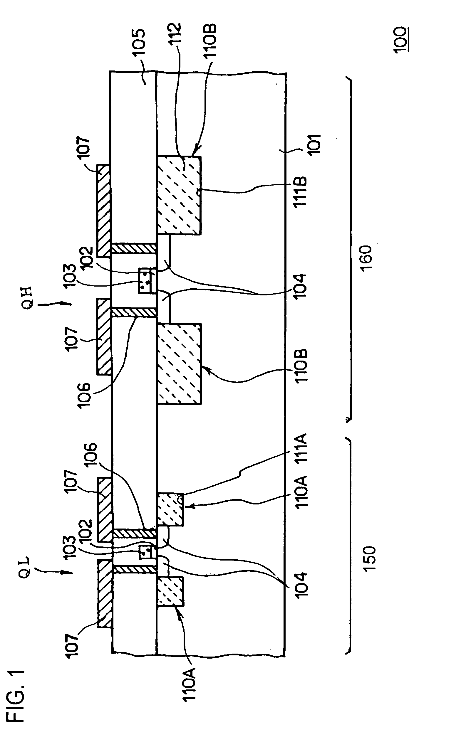
[0035] A semiconductor device according to the present embodiment will be described in reference to the annexed figures as follows. FIG. 1 is a schematic cross-sectional view of a semiconductor device according to the present embodiment. The present embodiment illustrates an example of applying the present invention to a memory device 100, and a peripheral region 160 is provided in a portion of a silicon substrate 101 that is the semiconductor substrate, and a cell region 150 composed of a memory cell that is the cell device is provided in other portion thereof. A higher breakdown voltage resistance MOS transistor QH, which is the high breakdown voltage resistance device, is formed in the peripheral region 160, as a device that is driven at a source voltage equivalent to or higher than a source voltage for a device (not shown in the drawings) in the cell region 150 driven at a lower source voltage, and a cell MOS transistor QL is formed as a device that is driven at...

Example

Second Embodiment

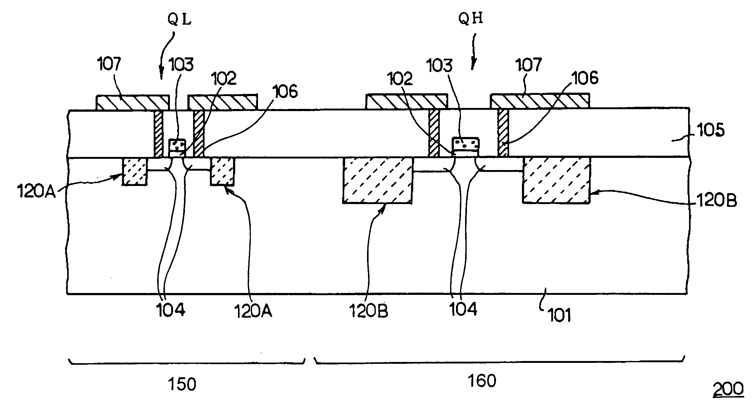
[0046] Next, a semiconductor device according to the present embodiment will be described in reference to the annexed figures as follows. FIG. 4 is a schematic cross-sectional view of a semiconductor device according to the present embodiment, and illustrates an example of applying the present invention to a memory device 200 similarly as in the first embodiment. As describing with assigning the same numeral for the equivalent element shown in the first embodiment, a peripheral region 160 is provided in a portion of a silicon substrate 101 and a cell region 150 composed of a memory cell is provided in other portion thereof. A higher breakdown voltage resistance MOS transistor QH is formed in the peripheral region 160, as a device that is driven at higher source voltage, and a cell MOS transistor QL is formed in the cell region 150, which is driven at lower source voltage than that of higher breakdown voltage resistance of MOS transistor QH. The structures of these ...

Example

Third Embodiment

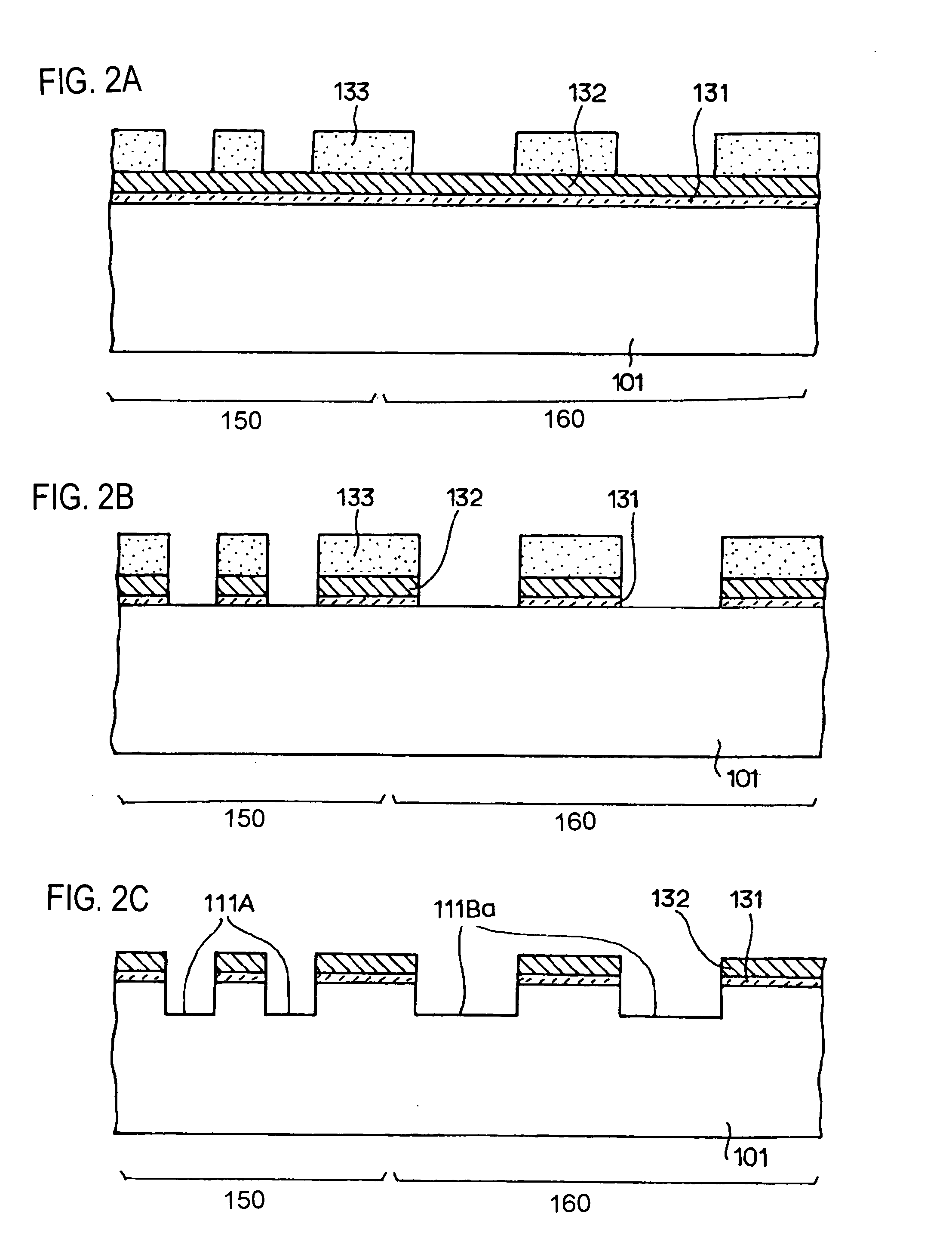
[0058]FIGS. 7A to 7D are cross sectional views, showing the process sequence of the method for manufacturing the memory device shown in FIG. 1 according to the present embodiment, which is manufactured by a different process from the process described in the first embodiment. First, as shown in FIG. 7A, a thin silicon oxide film 131 having a thickness of about 10 nm is formed on the surface of the silicon substrate 101 via a first oxidation process, and a silicon nitride film 132 having a thickness of about 150 nm is formed thereon via a nitridation process. Then, a first photo resist pattern 133A having openings disposed only in the locations for forming STI in the cell region 150 is formed on the silicon nitride film 132. The opening widths of the windows in the first photo resist pattern 133A are about 150 nm. Then, the silicon nitride film 132 and the silicon oxide film 131 are sequentially etched off thorough a mask of the first photo resist pattern 133A via a ...


PUM


Abstract

The present invention provides a technology for forming the trenches having different depths in one semiconductor substrate, which enables easily conducting the photo resist process employed for the etch process and forming trenches at higher depth dimension accuracy. The openings of the first films are formed in the semiconductor substrate to expose surfaces of the semiconductor substrate, the semiconductor substrate is etched through the openings to a depth of the shallower trench and then the cell region is covered with the second photo resist pattern, and the peripheral region is etched through the first films to form the deeper trench. Since the etch process is conducted under the conditions, in which the surfaces of the semiconductor substrate are exposed (opened) within the openings in the first film, trenches having different depths can be formed with higher depth dimension accuracy by suitably controlling the etch conditions.

Description

[0001] This application is based on Japanese Patent Application NO.2003-431807, the content of which is incorporated hereinto by reference. BACKGROUND OF THE INVENTION [0002] 1. Field of the Invention [0003] The present invention relates to a semiconductor device comprising a shallower trench and a deeper trench in one semiconductor substrate, and more particularly relates to a method for manufacturing a semiconductor device, which enables to form a shallow trench with higher depth dimension accuracy. [0004] 2. Related Art [0005] In semiconductor devices such as memory and the like, a cell region and a peripheral region are typically disposed on one semiconductor substrate, and these regions are driven at different voltages. In such semiconductor device, a device isolation insulating film for isolating devices formed in each of the regions is required to be designed corresponding to the driving voltages. More specifically, in the peripheral region utilizing higher driving voltage, t...

Claims


Application Information

Patent Timeline
IPC IPC(8): H01L21/3065H01L21/76H01L21/762H01L21/768H01L21/8242H01L27/08H01L27/10H01L27/108
CPCH01L21/76229
Inventor OTSUKI, KAZUTAKA
Owner NEC ELECTRONICS CORP
Why Eureka
Try Eureka