Semiconductor light emitting device having quantum well layer sandwiched between carrier confinement layers

a light-emitting device and quantum well technology, applied in the direction of solid-state devices, lasers, semiconductor lasers, etc., can solve the problems of considerable reduction of light-emitting output, and achieve the effect of improving the quality of each layer formed on the support substrate and raising the cutoff frequency

Inactive Publication Date: 2005-07-07
STANLEY ELECTRIC CO LTD
View PDF2 Cites 19 Cited by
  • Summary
  • Abstract
  • Description
  • Claims
  • Application Information

AI Technical Summary

Benefits of technology

[0012] By using such a support substrate, the quality of each layer to be formed on the support substrate can be improved and a cutoff frequency can be raised without lowering a light emission output.

Problems solved by technology

However, if the Zn concentration is increased, a light emission output lowers considerably.

Method used


Image

  • Semiconductor light emitting device having quantum well layer sandwiched between carrier confinement layers
  • Semiconductor light emitting device having quantum well layer sandwiched between carrier confinement layers
  • Semiconductor light emitting device having quantum well layer sandwiched between carrier confinement layers

Examples


first embodiment

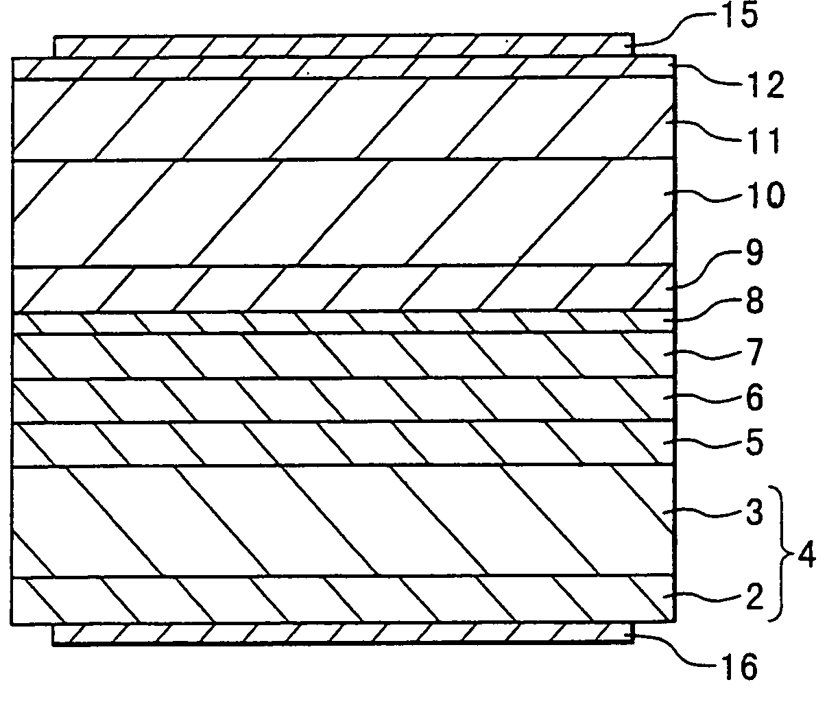
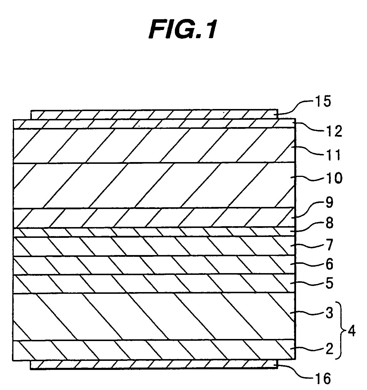
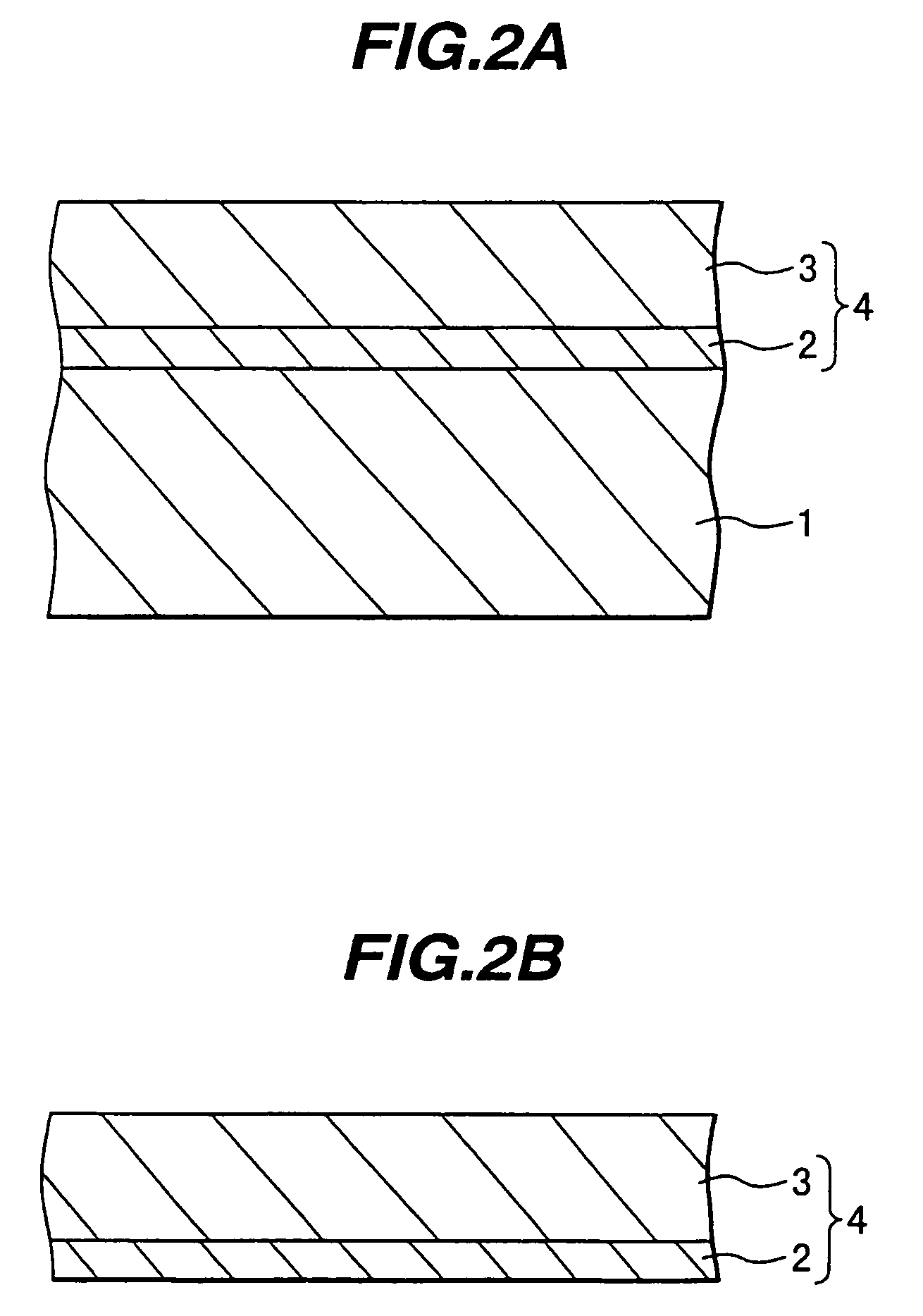
[0037]FIG. 1 is a cross sectional view of a semiconductor light emitting device according to the invention. A support substrate 4 is made of a high concentration layer 2 and a low concentration layer 3. The support substrate 4 is made of Zn doped p-type Al0.26Ga0.74As. The Zn concentration of the high concentration layer 2 is 1×1018 cm−3 and the Zn concentration of the low concentration layer 3 is 5×1017 cm−3. A thickness of the high concentration layer 2 is 40 μm and a thickness of the low concentration layer 3 is 110 μm.

[0038] On the surface of the low concentration layer 3, layers from an AlGaAs buffer layer 5 to a GaAs contact layer 12 are formed by metal organic chemical vapor deposition (MOCVD). The buffer layer 5 is made of Zn doped p-type Al0.26Ga0.74As and has a thickness of 0.2 μm and a Zn concentration of 1×1018 cm−3.

[0039] A lower clad layer 6 is made of Zn doped p-type Al0.32Ga0.68As and has a thickness of 0.5 μm and a Zn concentration of 1×1018 cm−3. A lower carrier c...

second embodiment

[0097] In the second embodiment, evaluations were conducted for the steepness of a composition change at the interface between the InGaAs strain quantum well layer and GaAs barrier layer formed on a GaAs substrate.

[0098]FIG. 14 is a cross sectional view of an evaluation sample. The principal surface of a GaAs substrate 20 is formed with a GaAs buffer layer 21 of 0.2 μm thick by MOCVD. The surface of the buffer layer 21 is stacked with five cycles of a two-layer structure of an InGaAs strain quantum well layer 22 of 10 nm thick and a GaAs barrier layer 23 of 20 nm thick.

[0099] A plurality of samples were prepared which were subjected to different growth temperatures and had different In composition ratios of the strain quantum well layers 22 and different crystalline orientations of principal surfaces of the GaAs substrates 20. The growth temperature is one of 620°C., 650° C. and 700° C. The In composition ratio of the strain quantum well layer 22 is 0.12 or 0.18. The principal surf...

third embodiment

[0108]FIG. 17 is a cross sectional view of a sample manufactured for the The principal surface of a GaAs substrate 30 is formed with a GaAs buffer layer 31 of 0.2 μm thick. Stacked on this buffer layer 31 are a lower clad layer 32, a lower carrier confinement layer 33, a strain quantum well layer 34, an upper carrier confinement layer 35, an upper clad layer 36 and a cap layer 37 in this order from the bottom. These layers were formed by MOCVD at the growth temperature of 650° C.

[0109] The lower and upper clad layers 32 and 36 are both made of Al0.39Ga0.61As and their thicknesses are 1 μm and 150 nm, respectively. The lower and upper carrier confinement layers 33 and 35 are both made of Al0.26Ga0.74As and their thicknesses are 50 nm. The strain quantum well layer 34 is made of InGaAs and its composition ratios and thickness change with each sample. The cap layer 37 is made of GaAs and has a thickness of 50 nm.

[0110]FIG. 18 shows the In composition ratio and thickness of the strain...


PUM


Abstract

The principal surface of a substrate made of a group III-V compound semiconductor material is about a (100) plane. A light emitting lamination structure is disposed on the principal surface. In the light emitting lamination structure, a quantum well layer is sandwiched by a pair of carrier confinement layers made of a semiconductor material having a band gap wider than a semiconductor material of the quantum well layer. The pair of carrier confinement layers are sandwiched by a pair of clad layers made of a semiconductor material having a band gap wider than the band gap of the semiconductor material of the carrier confinement layers. Thicknesses of the quantum well layer and the carrier confinement layers, as well as compositions of the semiconductor materials thereof, are set such that light emission recombination of electrons and holes occurs in the quantum well layer and not in the carrier confinement layers.

Description

CROSS REFERENCE TO RELATED APPLICATION [0001] The present application is a Divisional Application of U.S. application Ser. No. 10 / 664,659, which is based upon and claims the benefit of priority from and / or is related to prior Japanese Patent Application No. 2001-150610 filed on May 21, 2001 and Japanese Patent Application No. 2002-308171 filed on Oct. 23, 2002, the entire contents of which are incorporated herein by reference.BACKGROUND OF THE INVENTION [0002] A) Field of the Invention [0003] The present invention relates to a semiconductor light emitting device, and more particularly to a semiconductor light emitting device which is suitable for light emission in the wavelength band providing a high reception sensitivity of a photodiode using silicon and is capable of both increasing a light emission output and raising a cutoff frequency. [0004] B) Description of the Related Art [0005] A double-hetero type light emitting diode having a Zn doped GaAs layer sandwiched between AlGaAs ...

Claims


Application Information

Patent Timeline
Patent Type & Authority Applications(United States)
IPC IPC(8): H01L33/06H01L33/16H01L33/22H01L33/30H01L33/40
CPCB82Y20/00H01L33/30H01L33/06
Inventor MARUYAMA, TSUYOSHIISHII, KAZUHISASASAKURA, KENTOMITA, SHOTAROKAWAGUCHI, KEIZOTOMIYOSHI, TOSHIO
Owner STANLEY ELECTRIC CO LTD
Why Eureka
Try Eureka