Semiconductor device

a technology of heterojunction and semiconductor, applied in the direction of semiconductor devices, basic electric elements, electrical equipment, etc., can solve the problems of more likely avalanche breakdown, and more likely breakdown, so as to reduce the generation rate of carriers, prevent the occurrence of avalanche breakdown, and improve the breakdown voltage

Active Publication Date: 2005-07-07
PANASONIC SEMICON SOLUTIONS CO LTD
View PDF7 Cites 8 Cited by
  • Summary
  • Abstract
  • Description
  • Claims
  • Application Information

AI Technical Summary

Benefits of technology

[0026] Consequently, the carrier generation rate is reduced and the occurrence of the avalanche breakdown is prevented so that a semiconductor device having further improved breakdown voltage on high power output can be realized.
[0027] As is clear from the above explanation, the semiconductor device according to the present invention can realize a heterojunction bipolar transistor having the improved breakdown voltage on high power output.
[0028] Accordingly, the present invention makes it possible to provide the heterojunction bipolar transistor having the improved breakdown voltage on high power output. As a result, it is possible to realize a heterojunction bipolar transistor that can be commercially utilized as a power device of a terminal transmitter of the GSM system. Therefore, its practical value is very high.

Problems solved by technology

Accordingly, the more the number of carriers increases, the more likely the avalanche breakdown occurs.
In addition, the stronger the intensity of the electric field is, the more likely the avalanche breakdown occurs.
However, the conventional HBT as shown in FIG. 2B has a problem that a breakdown is likely to occur as Ic increases.

Method used


Image

  • Semiconductor device
  • Semiconductor device
  • Semiconductor device

Examples


Embodiment Construction

[0044] The following explains about a semiconductor device according to the embodiment of the present invention with reference to diagrams.

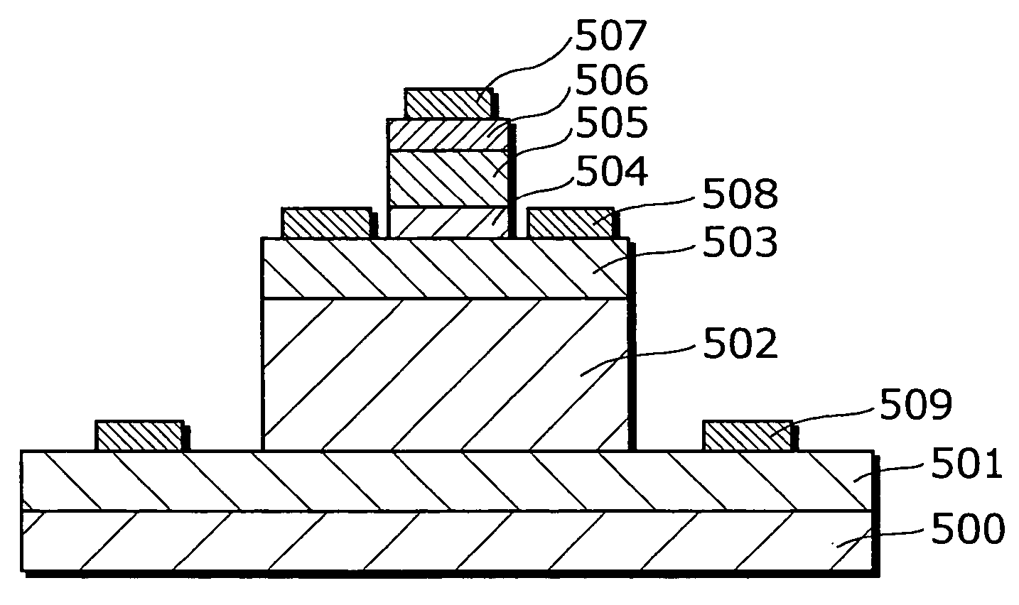
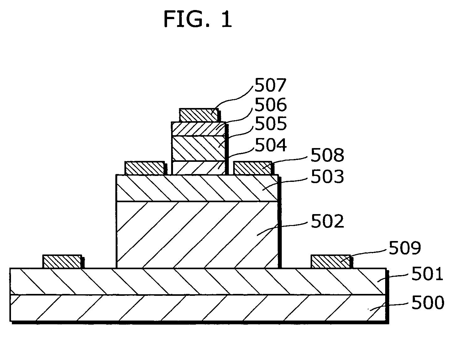
[0045]FIG. 5 is a cross-section diagram showing a device structure of a HBT in the present embodiment.

[0046] The HBT in the present embodiment is aimed to realize a HBT having an improved breakdown voltage on high power output. In the HBT, the following layers are sequentially laminated on a semi-insulating GaAs substrate 100, by a crystal growth using a MOCVD method (Metal Organic Chemical Vapor Depoint method) or a MBE method (Molecular-Beam Epitaxial method), the layers being a n-type GaAs subcollector layer 101 with a thickness of 6000Å formed by doping n-type impurities at a concentration of 4×1018 cm−3, a n-type GaAs intermediate collector layer 102, a n-type GaAs collector layer 103 with a thickness of 4500Å formed by doping n-type impurities at a concentration of 1×1016 cm−3, a p-type GaAs base layer 104, a n-type InGaP second emitter l...


PUM


Abstract

It is the object of the present invention to provide a semiconductor device having an improved breakdown voltage on high power output, the semiconductor device comprising a n-type GaAs subcollector layer 101, a n-type GaAs intermediate collector layer 102 formed between a collector layer 103 and the subcollector layer 101, the n-type GaAs collector layer 103, a p-type GaAs base layer 104, a n-type InGaP second emitter layer 105, a n-type GaAs first emitter layer 106, and a n-type InGaAs emitter contact layer 107, and a concentration of impurities in the intermediate collector layer 102 is higher than a concentration of impurities in the collector layer 103 and is lower than a concentration of impurities in the subcollector layer 101.

Description

BACKGROUND OF THE INVENTION [0001] (1) Field of the Invention [0002] The present invention relates to a heterojunction bipolar transistor which has been widely used for a communication transmitting high power amplifier. [0003] (2) Description of the Related Art [0004] Conventionally, a compound semiconductor device such as a Field-Effect Transistor (hereafter referred to as FET) and a Heterojunction Bipolar Transistor (hereafter referred to as HBT) have been used for a communication transmitting high power amplifier that is one of the components of a cellular phone, and the like. [0005]FIG. 1 is a cross-section diagram showing a device structure of a typical conventional HBT (e.g. refer to Japanese Laid-Open Patent Publication No. 2001-326231). [0006] As shown in FIG. 1, in the conventional HBT, by a crystal growth using a MOCVD method (Metal Organic Chemical Vapor Depoint method) or a MBE method (Molecular-Beam Epitaxial method), the following layers are sequentially laminated on a...

Claims


Application Information

Patent Timeline
Patent Type & Authority Applications(United States)
IPC IPC(8): H01L21/331H01L29/737
CPCH01L29/7371H01L29/0821
Inventor NOGOME, MASANOBUTAMURA, AKIYOSHIMURAYAMA, KEIICHI
Owner PANASONIC SEMICON SOLUTIONS CO LTD
Why Eureka
Try Eureka