Semiconductor sensor device and method of producing the same

a semiconductor sensor and sensor technology, applied in the direction of acceleration measurement using interia forces, acceleration measurement in multiple dimensions, instruments, etc., can solve the problems of difficult to produce a semiconductor sensor device with a high reliability, external noise easily entering the bonding wires, etc., and achieve the effect of adjusting the output characteristics

Inactive Publication Date: 2005-07-07
RICOH KK
View PDF10 Cites 16 Cited by
  • Summary
  • Abstract
  • Description
  • Claims
  • Application Information

AI Technical Summary

Benefits of technology

[0017] In a case where the method of producing the semiconductor sensor device further comprises the steps of (d) inspecting output characteristics of the semiconductor sensor devices after the step (b) and before the step (c); and (e) adjusting the output characteristics of the semiconductor sensor devices by adjusting resistances in the signal processing IC chips via the trimming windows based on inspection results of the step (d), and the step (g) is carried out after the step (e), the resin encapsulation of the periphery of the signal processing IC chip and the resin encapsulation of the trimming windows may be carried out simultaneously. However, when carrying out the step (g) before the step (e), the resin encapsulation of the formation region of the trimming windows should be avoided.
[0018] It is possible to provide a step of forming a dam member in the semiconductor sensor chip region of the semiconductor wafer so as to surround the semiconductor sensor formation region and / or a dam member surrounding on the signal processing IC chip so as to surround the semiconductor sensor formation region, prior to the step (g). In this case, it is possible to prevent the encapsulating resin from entering the space between the signal processing IC chip and the semiconductor sensor chip on the inner side of the dam member.

Problems solved by technology

For this reason, there were problems in that external noise easily enter the bonding wires, and that it is difficult to produce a semiconductor sensor device having a high reliability.

Method used


Image

  • Semiconductor sensor device and method of producing the same
  • Semiconductor sensor device and method of producing the same
  • Semiconductor sensor device and method of producing the same

Examples


first embodiment

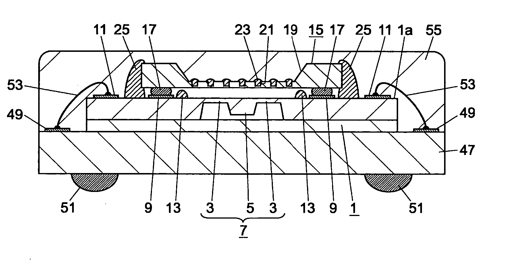
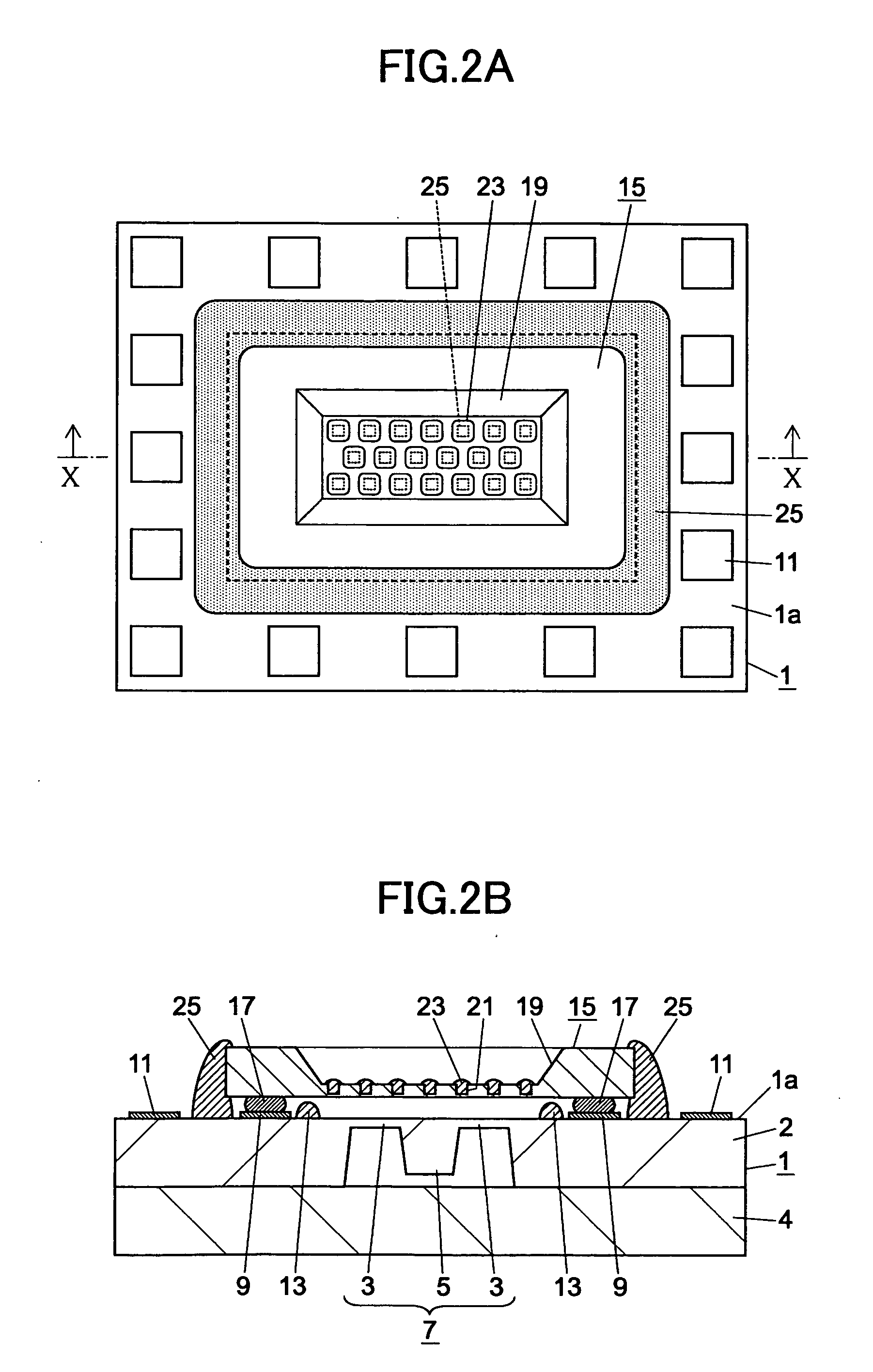
[0035]FIGS. 2A and 2B respectively are a plan view and a cross sectional view generally showing a semiconductor sensor device according to the present invention. FIG. 2B shows the cross section cut along a line X-X in FIG. 2A.

[0036] A semiconductor sensor chip 1 shown in FIGS. 2A and 2B is made up of a silicon substrate 2 having a planar size of 2.5 mm×2.5 mm and a thickness of 400 μm, for example, and a glass base (or seat) 4. The silicon substrate 2 and the glass base 4 are bonded by anodic bonding, for example. A diaphragm part 3 is formed on a surface 1a of the silicon substrate 2, and a weight 5 is formed at a central portion of the diaphragm part 3. Piezoresistance elements (not shown) and electrodes (not shown) are formed on the diaphragm part 3 on the periphery of the weight 5, so as to form a piezoresistance type 3-axis semiconductor acceleration sensor (hereinafter simply referred to as a semiconductor sensor) 7. A formation region of the semiconductor sensor 7 has a plana...

fourth embodiment

[0066]FIG. 9 is a cross sectional view generally showing the semiconductor sensor device according to the present invention. In FIG. 9, those parts which are the same as those corresponding parts in FIGS. 2A and 2B are designated by the same reference numerals, and a description thereof will be omitted.

[0067] In FIG. 9, a BGA 35 has an IC chip 39 mounted on a wiring substrate 37, and pad electrodes 41 provided on a peripheral part of the wiring substrate 37 are electrically connected to pad electrodes 43 provided on the IC chip 39 by bonding wires 45. A resistor circuit for resistance adjustment and fuse elements are formed inside the IC chip 39, and the trimming windows 21 are formed in a top surface of the IC chip 39 in correspondence with the positions where the fuse elements are formed. The encapsulating resin 23 fills the trimming windows 21. Wiring patterns (not shown) which connect to the pad electrodes 41 are formed on the wiring substrate 37, and penetrating holes (not show...


PUM

PropertyMeasurementUnit
thicknessaaaaaaaaaa
sizeaaaaaaaaaa
sizeaaaaaaaaaa

Abstract

A semiconductor sensor device is provided with a semiconductor sensor chip having a plurality of electrodes formed on a substrate surface and a semiconductor sensor, and a signal processing IC chip mounted on the semiconductor sensor chip by flip-chip bonding.

Description

BACKGROUND OF THE INVENTION [0001] This application claims the benefit of a Japanese Patent Application No.2003-417509 filed Dec. 16, 2003, in the Japanese Patent Office, the disclosure of which is hereby incorporated by reference. [0002] 1. Field of the Invention [0003] The present invention generally relates to, and more particularly to semiconductor sensor devices and methods of producing the same, and more particularly to a semiconductor sensor device which is provided with a semiconductor sensor chip having a semiconductor sensor such as a semiconductor pressure sensor, semiconductor acceleration sensor and semiconductor angular velocity sensor, and a signal processing integrated circuit (IC) chip having an amplifier for amplifying an output of the semiconductor sensor and the like, and to a method of producing such a semiconductor sensor device. [0004] 2. Description of the Related Art [0005] Semiconductor sensors, such as semiconductor pressure sensors, semiconductor accelera...

Claims


Application Information

Patent Timeline
Patent Type & Authority Applications(United States)
IPC IPC(8): G01L9/00G01P1/02G01P15/08G01P15/12H01L23/48H01L25/16H01L29/84
CPCG01L19/148G01P1/023G01P15/0802G01P15/123G01P15/18H01L25/16H01L2224/48137H01L2924/10253H01L2924/14H01L2924/30107H01L2924/01019H01L2924/00H01L2224/05554H01L2924/181G01P2015/084H01L2924/00012
Inventor SETO, MASAMI
Owner RICOH KK
Why Eureka
Try Eureka