Method of preventing surface roughening during hydrogen prebake of SiGe substrates

Inactive Publication Date: 2005-07-07
IBM CORP
View PDF10 Cites 84 Cited by
  • Summary
  • Abstract
  • Description
  • Claims
  • Application Information

AI Technical Summary

Benefits of technology

[0006] The invention forms an epitaxial Si layer on a SiGe surface, and avoids creating a rough surface upon which the epitaxial Si layer is grown. In order to avoid creating the rough surface, the invention first performs an HF etching process on the SiGe surface. This etching process removes most of the oxide from the surface, and leaves a first amount of oxygen (typically a dose of 1×10¹³-1×10¹⁵/cm2 oxygen) on the SiGe surface. The invention then performs a hydrogen pre-bak

Problems solved by technology

Additionally, if the active region of an electrical device fabricated on the substrate is close to the epitax

Method used


Image

  • Method of preventing surface roughening during hydrogen prebake of SiGe substrates
  • Method of preventing surface roughening during hydrogen prebake of SiGe substrates
  • Method of preventing surface roughening during hydrogen prebake of SiGe substrates

Examples


Embodiment Construction

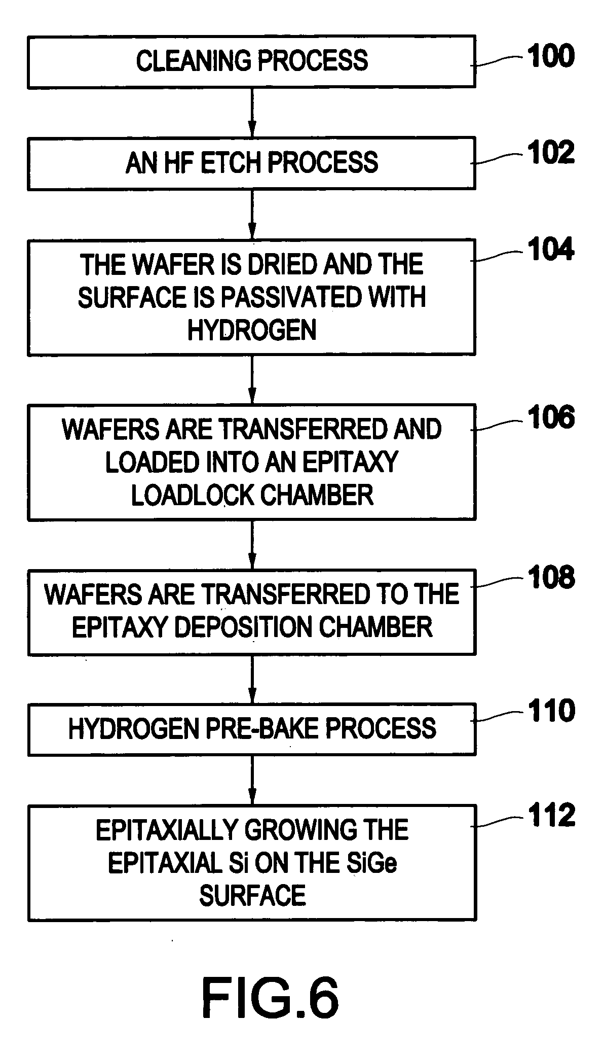
[0016] The present invention and the various features and advantageous details thereof are explained more fully with reference to the nonlimiting embodiments that are detailed in the following description. Descriptions of well-known components and processing techniques are omitted so as to not unnecessarily obscure the present invention. The examples used herein are intended merely to facilitate an understanding of ways in which the invention may be practiced and to further enable those of skill in the art to practice the invention. Accordingly, the examples should not be construed as limiting the scope of the invention.

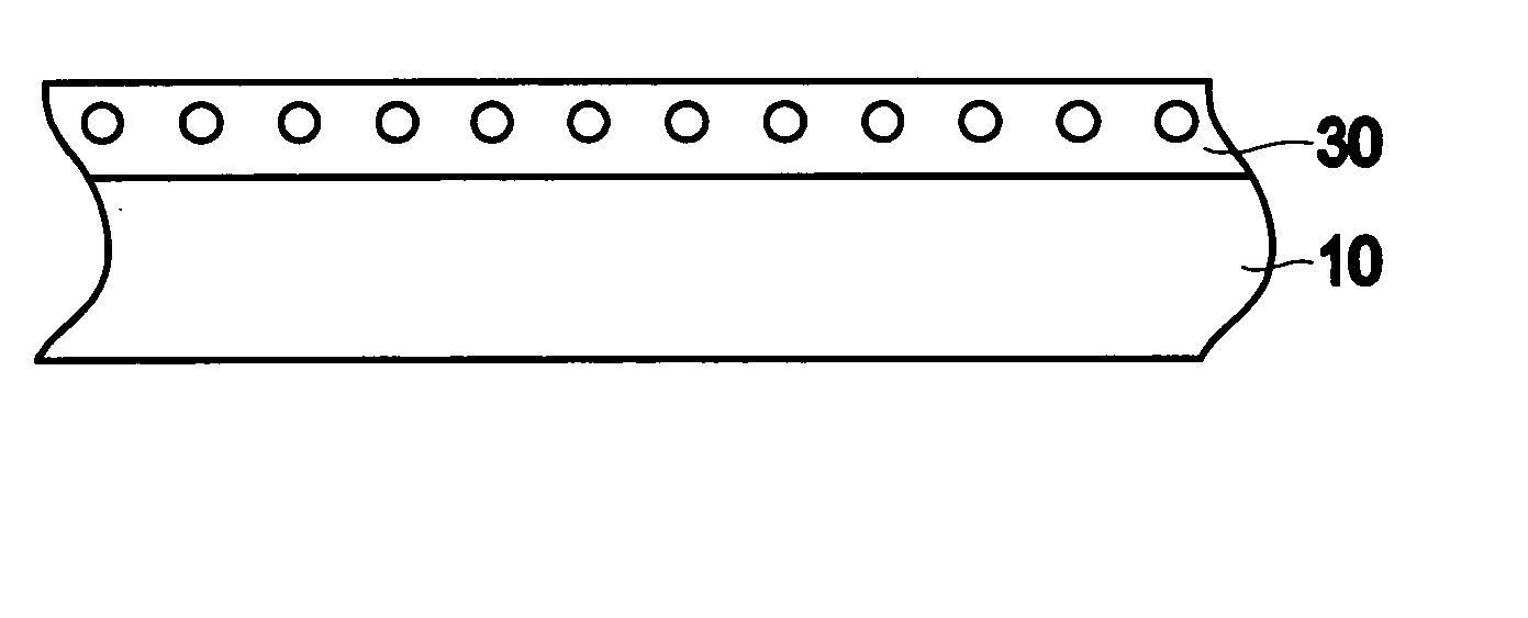
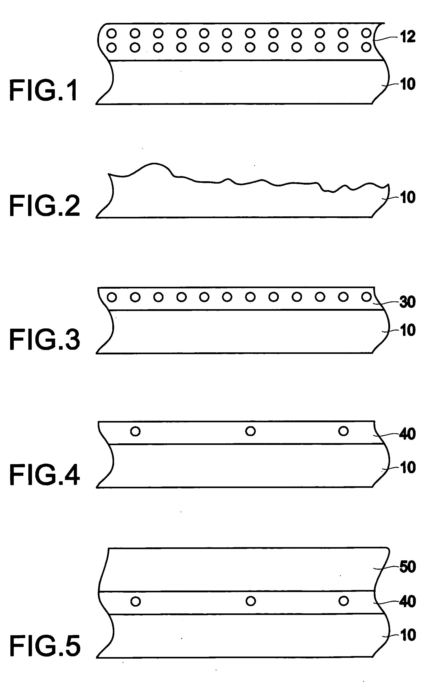
[0017] The present invention generally relates to Si epitaxy on a SiGe surfaces that are normally coated with a thin oxide after experiencing an ambient environment. In epitaxial processes, it is important to reduce the amount of oxide on the substrate for a high quality epitaxial film to be grown. If the surface oxygen content is high enough, it will detrimentally ...


PUM


Abstract

The invention forms an epitaxial silicon-containing layer on a silicon germanium, patterned strained silicon, or patterned thin silicon-on-insulator surface and avoids creating a rough surface upon which the epitaxial silicon-containing layer is grown. In order to avoid creating the rough surface, the invention first performs a hydrofluoric acid etching process on the silicon germanium, patterned strained silicon, or patterned thin silicon-on-insulator surface. This etching process removes most of oxide from the surface, and leaves a first amount of oxygen (typically 1×10¹³-1×10¹⁵/cm2 of oxygen) on the silicon germanium, patterned strained silicon, or patterned thin silicon-on-insulator surface. The invention then performs a hydrogen pre-bake process which heats the silicon germanium, patterned strained silicon, or patterned thin silicon-on-insulator surface sufficiently to remove additional oxygen from the surface and leave a second amount of oxygen, less than the first amount, on the silicon germanium, patterned strained silicon, or patterned thin silicon-on-insulator surface. The heating process leaves an amount of at least 5×10¹²/cm2 of oxygen (typically, between approximately 1×10¹³/cm2 and approximately 5×10¹³/cm2 of oxygen) on the silicon germanium, patterned strained silicon, or patterned thin silicon-on-insulator surface. By leaving a small amount of oxygen on the silicon germanium, patterned strained silicon, or patterned silicon-on-insulator surface, the heating processes avoid changing the roughness of the silicon germanium, patterned strained silicon, or patterned thin silicon-on-insulator surface. Then the process of epitaxially growing the epitaxial silicon-containing layer on the silicon germanium, patterned strained silicon, or patterned silicon-on-insulator surface is performed.

Description

CROSS-REFERENCE TO RELATED APPLICATION [0001] The present application is related to a new U.S. Patent Application, filed concurrently, to Chen et al., entitled “A METHOD OF PREVENTING SURFACE ROUGHENING DURING HYDROGEN PRE-BAKE OF SIGE SUBSTRATES USING CHLORINE CONTAINING GASES”, having (IBM) Docket No. FIS920030350US1, assigned to the present assignee, and incorporated herein by reference.BACKGROUND OF THE INVENTION [0002] 1. Field of the Invention [0003] The invention generally relates to the growth of epitaxial silicon (Si) or silicon germanium (SixGe1-x, for simplicity, we use SiGe in the following description) on various semiconductor crystal surfaces and more particularly to an improved method that reduces the amount of oxygen on the semiconductor crystal surfaces, without roughening the surfaces. [0004] 2. Description of the Related Art [0005] The surfaces of Si wafers normally become covered with a thin native oxide layer when exposed for more than a few minutes in an oxygen...

Claims


Application Information

Patent Timeline
IPC IPC(8): C30B25/02C30B29/06C30B29/52H01L21/20H01L21/205H01L21/28H01L21/306H01L21/3205H01L21/36H01L21/44
CPCC30B25/02C30B29/06C30B29/52H01L21/02046H01L21/02052H01L21/02658H01L21/0243H01L21/02661H01L21/02381H01L21/02532Y10S438/933
Inventor CHEN, HUAJIEMOCUTA, DAN M.MURPHY, RICHARD J.BEDELL, STEPHAN W.SADANA, DEVENDRA K.
Owner IBM CORP
Why Eureka
Try Eureka