

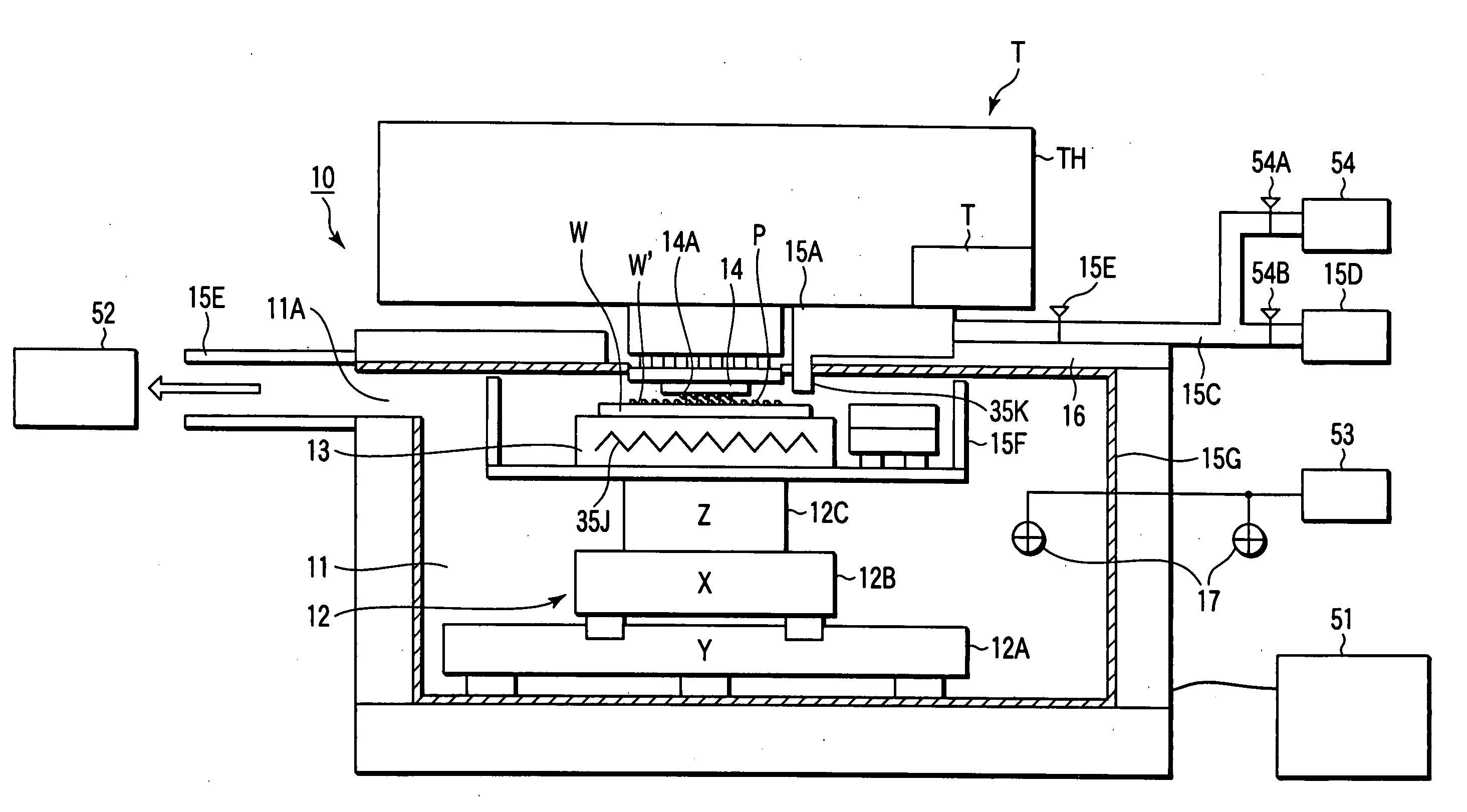
Probe method, prober, and electrode reducing/plasma-etching processing mechanism
a technology of reducing/plasmaetching and probe pins, which is applied in the direction of electronic circuit testing, measurement devices, instruments, etc., can solve the problems of undesired change of electrical characteristics of semiconductor products, inability to apply test signals to the electrodes of the tester, and inability to electrically connect the electrodes to the probe pins, etc., to achieve the effect of reducing the damage to the target obj
- Summary
- Abstract
- Description
- Claims
- Application Information
AI Technical Summary
Benefits of technology
Problems solved by technology
Method used
Image

Examples
example 1
[0098] In this example, the reducing performance of the forming gas was observed. The oxide film of a copper wafer (thin copper film=1 μm, TiN underlying layer=15 nm) (to be merely referred to as “reference wafer” hereinafter) for reference was reduced in a forming gas atmosphere. The oxygen concentration distribution in the thin copper film was observed. More specifically, the reference wafer was placed on a stage. The reference wafer was heated on the stage which was set at a temperature of 150° C. In this state, a forming gas (hydrogen gas concentration=3% by volume) was supplied to expose the reference wafer to the forming gas atmosphere. After that, the oxygen concentration distribution in the thin copper film was observed with an X-ray photoelectron spectroscope (XPS). In the same manner, while heating a reference wafer, only nitrogen gas was supplied to expose the reference wafer to a nitrogen gas atmosphere. After that, the oxygen concentration distribution in the thin coppe...
example 2
[0099] According to this example, the influence of the temperature of the stage when reducing the oxide film of a reference wafer by using a forming gas was observed. More specifically, as shown in FIG. 6, the temperature of the stage was changed between 250° C., 300° C., 325° C., and 350° C., and the oxygen concentration distribution in the thin copper film at each temperature was observed with the XPS. FIG. 6 shows the results of this observation. According to the results shown in FIG. 6, the higher the temperature of the stage, the more the reduction was promoted.
example 3
[0100] In this example, the influence of humidity on oxidation was observed. More specifically, wafers were left in dry air (dew point: −70° C.), an atmosphere (temperature=25° C., humidity=50%), and nitrogen gas for time periods shown in FIG. 7A. The progress of oxidation of the copper wafers (thin copper film=1 μm, TiN underlying layer=15 nm) in the respective atmospheres were observed. FIG. 7A shows the results of this observation. Oxidation rates in dry air and in atmosphere were obtained. FIG. 7B shows the obtained results. Marks ♦ in FIG. 7A indicate the oxygen concentration distribution in the thin copper film immediately after the copper wafer was fabricated. According to the results shown in FIGS. 7A and 7B, the longer the leaving time in a high-humidity atmosphere, the more the oxidation of the thin copper film progressed, and the larger the thickness of the oxide film to be reduced. In contrast to this, in the dry air, even when the leaving time was long, oxidation did no...
PUM
| Property | Measurement | Unit |
|---|---|---|
| temperature | aaaaa | aaaaa |
| temperature | aaaaa | aaaaa |
| temperature | aaaaa | aaaaa |
Abstract
Description
Claims
Application Information