Triangular conforming transmission structure

a transmission structure and triangular technology, applied in the direction of conductive pattern formation, waveguides, high frequency circuit adaptations, etc., can solve the problems of reducing bandwidth, difficult to achieve the desired uniformity within the system, and simply limited in their electronic performance primarily by their structure, so as to reduce or eliminate the impedance discontinuities at the “triad” connector/transmission line interfa

Inactive Publication Date: 2005-07-14
MOLEX INC
View PDF22 Cites 18 Cited by
  • Summary
  • Abstract
  • Description
  • Claims
  • Application Information

AI Technical Summary

Benefits of technology

[0012] The present directed is therefore directed to an improved transmission structure that overcomes the aforementioned disadvantages and utilizes grouped electrically conductive elements to form a unitary mechanical structure that provides a complete electronic transmission channel that is similar in one sense to a fiber optic system. The focus of the invention is on providing a complete, engineered copper-based electronic transmission channel rather than utilizing either individual conductive pins or separable interfaces with copper conductors as the transmission channel, the transmission channels of the invention yielding more predictable electrical performance and greater control of operational characteristics. Such improved systems of the present invention are believed to offer operating speeds for digital signal transmission of up to at least 12.5 GHz at extended path lengths which are much greater than 0.25 inch.
[0015] A further object of the present invention is to control the impedance of the channel link by selectively sizing the conductive elements and the gaps therebetween on the exterior surface of the elongated body to maintain balanced or unbalanced electrical & magnetic fields.
[0018] A yet further object of the present invention is to provide an improved transmission line in the form of a solid link, of preferably uniform, circular cross-section, the link including at least a pair of conductive elements disposed thereon that serve to guide the electrical wave therethrough, the link including at least one thin filament of dielectric material having two conductive surfaces disposed thereon, the conductive surfaces extending lengthwise of the filament and separated by two circumferential arcuate extents, the conductive surfaces further being separated from each other to form a discrete, two-element transmission channel that reduces the current loop and in which the signal conductors are more tightly aligned.
[0020] The present invention accomplishes the above and other objects by virtue of its unique structure. In one principal aspect, the present invention includes a transmission line that is formed from a dielectric, through which conductors are spaced and arranged to conform to the aforementioned triangular conductor pattern of a “triad” connector. The triangular “triad” conductor pattern is accomplished by spacing the electrodes using a slot is cut or formed through dielectric. At the top edge of each side of the slot and just outside the slot, a thin, narrow strip of conductive material is deposited on each side of the slot. A thin strip of conductive material is deposited at the bottom of the slot. By sizing the depth and width of the slot, the transmission line conductors along the slot's top edges and the bottom can be precisely matched to the triangular spacing used in virtually any “triad” conductor. By matching the transmission line's conductors to a “triad” connector, impedance discontinuities at a “triad” connector / transmission line interface can be reduced or eliminated.

Problems solved by technology

Most, if not all of these transmission means, suffer from inherent speed limitations such as both the upper frequency limit and the actual time a signal requires to move from one point to another within the system, which is commonly referred to as propagation delay.
They simply are limited in their electronic performance primarily by their structure, and secondarily by their material composition.
It is difficult to achieve the desired uniformity within the system when the transmission system is constructed from individual pins.
Although satisfactory in performance at low operating speeds, at high operational speeds, these systems would consider the conductors as discontinuities in the system that affect the operation and speed thereof.
Many signal terminals or pins in these systems were connected to the same ground return conductor, and thus created a high signal to ground ratio, which did not lend themselves to high-speed signal transmission because large current loops are forced between the signals and the ground, which current loops reduce the bandwidth and increase the cross talk of the system, thereby possibly degrading the system performance.
However, as the transmission frequency increases, the reduction in size creates its own problem in that the effective physical length is reduced to rather small sizes.
High frequencies in the 10 Ghz range and above render most of the calculated system path lengths unacceptable.
In addition to aggregate inductance and capacitance across the system being limiting performance factors, any non-homogeneous geometrical and / or material transitions create discontinuities.
It can thus be seen that the evolution of electronic transmission structures have progressed from uniform-structured pin arrangements to functionally dedicated pins arrangements to attempted unitary structured interfaces, yet the path length and other factors still limit these structures.
With the aforementioned prior art structures, it was not feasible to carry high frequency signals due to the physical restraints of these systems and the short critical path lengths needed for such transmission.
This is very difficult to achieve when the delivery system is constructed from individual, conductive pins designed to interconnect with other individual conductive pins because of potential required changes in the size, shape and position of the pins / terminals with respect to each other.
These type of systems all are limited with respect to attaining the critical path lengths mentioned above.

Method used


Image

  • Triangular conforming transmission structure
  • Triangular conforming transmission structure
  • Triangular conforming transmission structure

Examples


Embodiment Construction

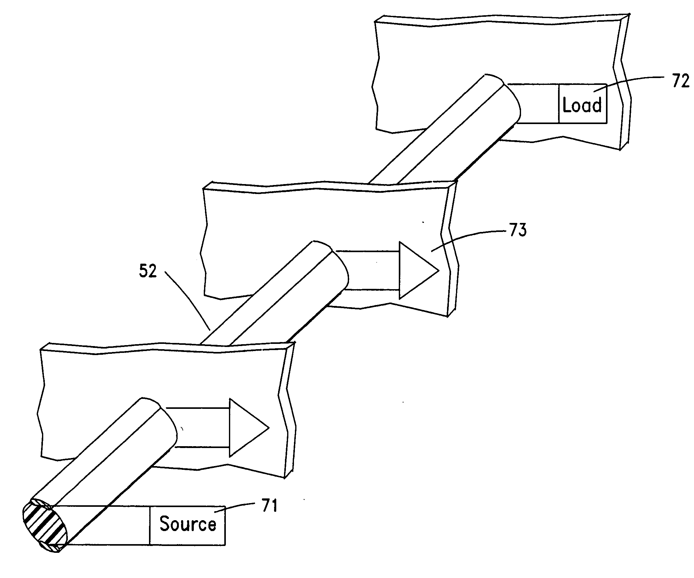
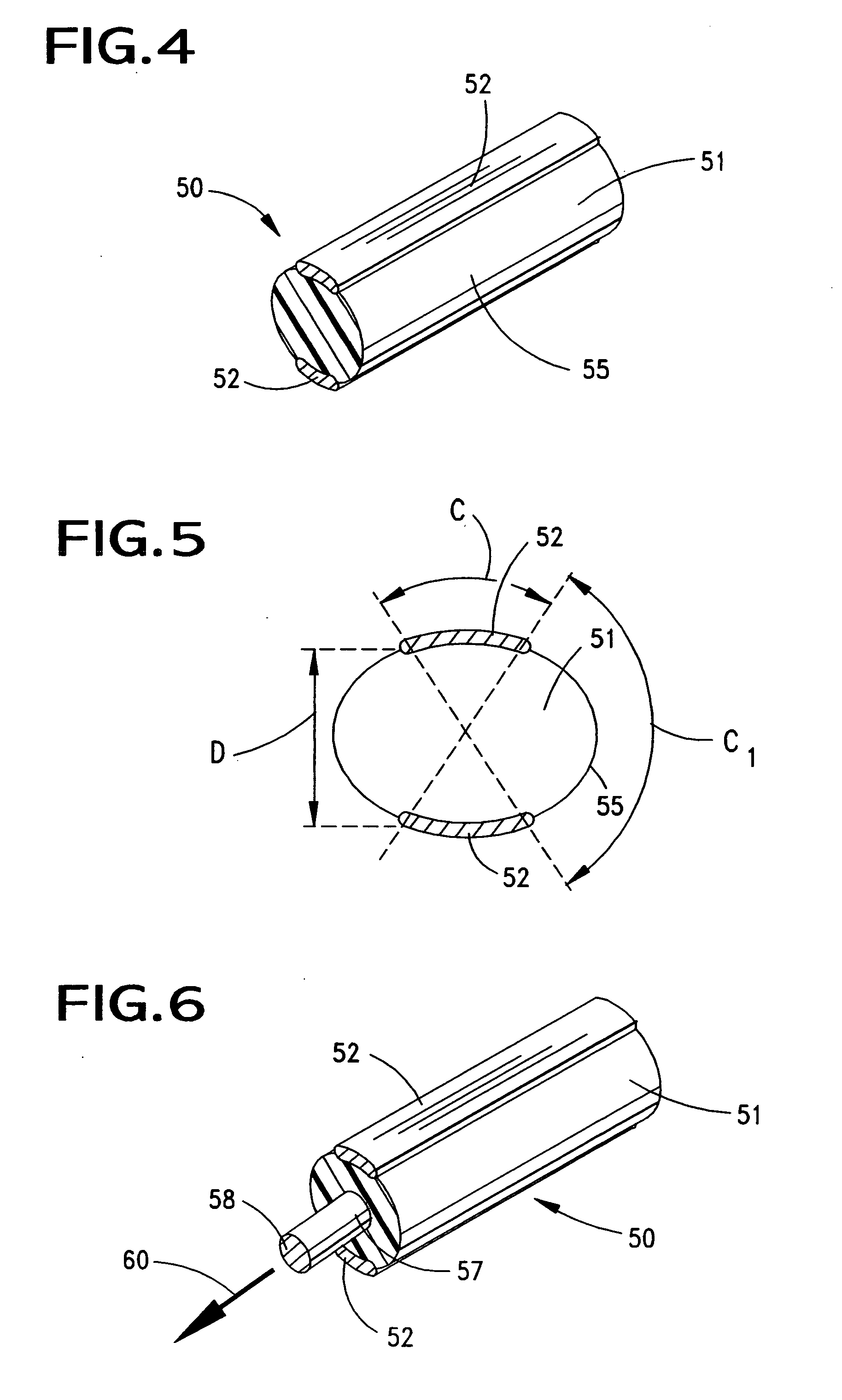
[0053]FIG. 4 illustrates a grouped element channel link 50 constructed in accordance with the principles of the present invention. It can be seen that the link 50 includes an elongated, dielectric body 51, preferably a cylindrical filament, that is similar to a length of fiber optic material. It differs therefrom in that the link 50 acts as a pre-engineered wave guide and a dedicated transmission media. In this regard, the body 51 is formed of a dedicated dielectric having a specific dielectric constant and a plurality of conductive elements 52 applied thereto. In FIGS. 4 and 5, the conductive elements 52 are illustrated as elongated extents, traces or strips, 52 of conductive material and, as such, they may be traditional copper or precious metal extents having a definite cross-section that may be molded or otherwise attached, such as by adhesive or other means to the dielectric body of the link 50. They may also be formed on the exterior surface 55 of the body 51 such as by a suit...


PUM


Abstract

A reduced-cross-sectional area, triad transmission line is formed by plating or metallizing surface area of a substrate, along the edge of a slot cut through the substrate. The cross-sectional area of such conductors that faces each other is reduced, reducing the signal coupling between them when they are carrying high-frequency signals. An intervening ground plane between them is provided by metallization on the slot bottom that is held at ground potential.

Description

REFERENCE TO RELATED APPLICATIONS [0001] This application claims priority of prior U.S. Provisional Patent Application No. 60 / 532,719, filed Dec. 24, 2004. BACKGROUND OF THE INVENTION [0002] The present invention pertains to multi-circuit electronic communication systems, and more particularly, to a dedicated transmission channel structure for use in such systems and which can be utilized in all parts of a transmission system, chip packaging, circuit board construction, interconnect devices and launches for such systems. [0003] Various means of electronic transmission are known in the art. Most, if not all of these transmission means, suffer from inherent speed limitations such as both the upper frequency limit and the actual time a signal requires to move from one point to another within the system, which is commonly referred to as propagation delay. They simply are limited in their electronic performance primarily by their structure, and secondarily by their material composition. ...

Claims


Application Information

Patent Timeline
Patent Type & Authority Applications(United States)
IPC IPC(8): H01P1/04H01P3/02H01R13/6461H01R13/6474H01R13/6477H01R13/658H01R13/6585H05K1/02H05K3/10
CPCH01P3/02H05K1/0219H05K2201/09236H05K3/107H05K2201/09036H05K1/024H01P1/04H01P3/08
Inventor BRUNKER, DAVID L.
Owner MOLEX INC
Why Eureka
Try Eureka