Novel shallow trench isolation method for reducing oxide thickness variations at different pattern densities

a shallow trench and oxide thickness technology, applied in the direction of basic electric elements, semiconductor/solid-state device manufacturing, electric devices, etc., can solve the problems of difficult correction, difficult to reduce, and difficult to reduce thickness variation, so as to reduce thickness variation

Active Publication Date: 2005-07-14
TAIWAN SEMICON MFG CO LTD
View PDF8 Cites 61 Cited by
  • Summary
  • Abstract
  • Description
  • Claims
  • Application Information

AI Technical Summary

Benefits of technology

[0010] An objective of the present invention is to provide a method of forming STI features with a different pattern density and with a reduced thickness variation in the dielectric layer that fills the shallow trenches.
[0011] Another objective of the present invention is to provide a method of forming STI features that does not decrease throughput or increase cost compared to an existing process.

Problems solved by technology

A subsequent planarization process involving a chemical mechanical polish (CMP) step cannot compensate for the thickness variation and causes a dishing or bowl shaped indentation in the insulating layer formed within wide shallow trenches.
The problem is not easily corrected and expensive rework steps may result.
However, the method is not applicable when the width of the active region shrinks to about 0.13 micron or less.
However, these prior art methods do not address the issue of different size trenches or trenches with different pattern densities that need to be filled to the same level.

Method used


Image

  • Novel shallow trench isolation method for reducing oxide thickness variations at different pattern densities
  • Novel shallow trench isolation method for reducing oxide thickness variations at different pattern densities
  • Novel shallow trench isolation method for reducing oxide thickness variations at different pattern densities

Examples


second embodiment

[0026] The present invention relates to a method of forming shallow trench isolation (STI) features with different pattern densities and with a uniform insulating layer thickness. The method is applicable to fabricating any device in which isolation regions are used to separate active regions on a substrate. In a second embodiment, the method may be used to form a uniform dielectric layer over a pattern of metal lines on a substrate. The drawings are for illustration only and are not intended to limit the scope of the invention. The figures are not necessarily drawn to scale and the relative sizes of the various features shown in the drawings may be different than those in an actual device.

first embodiment

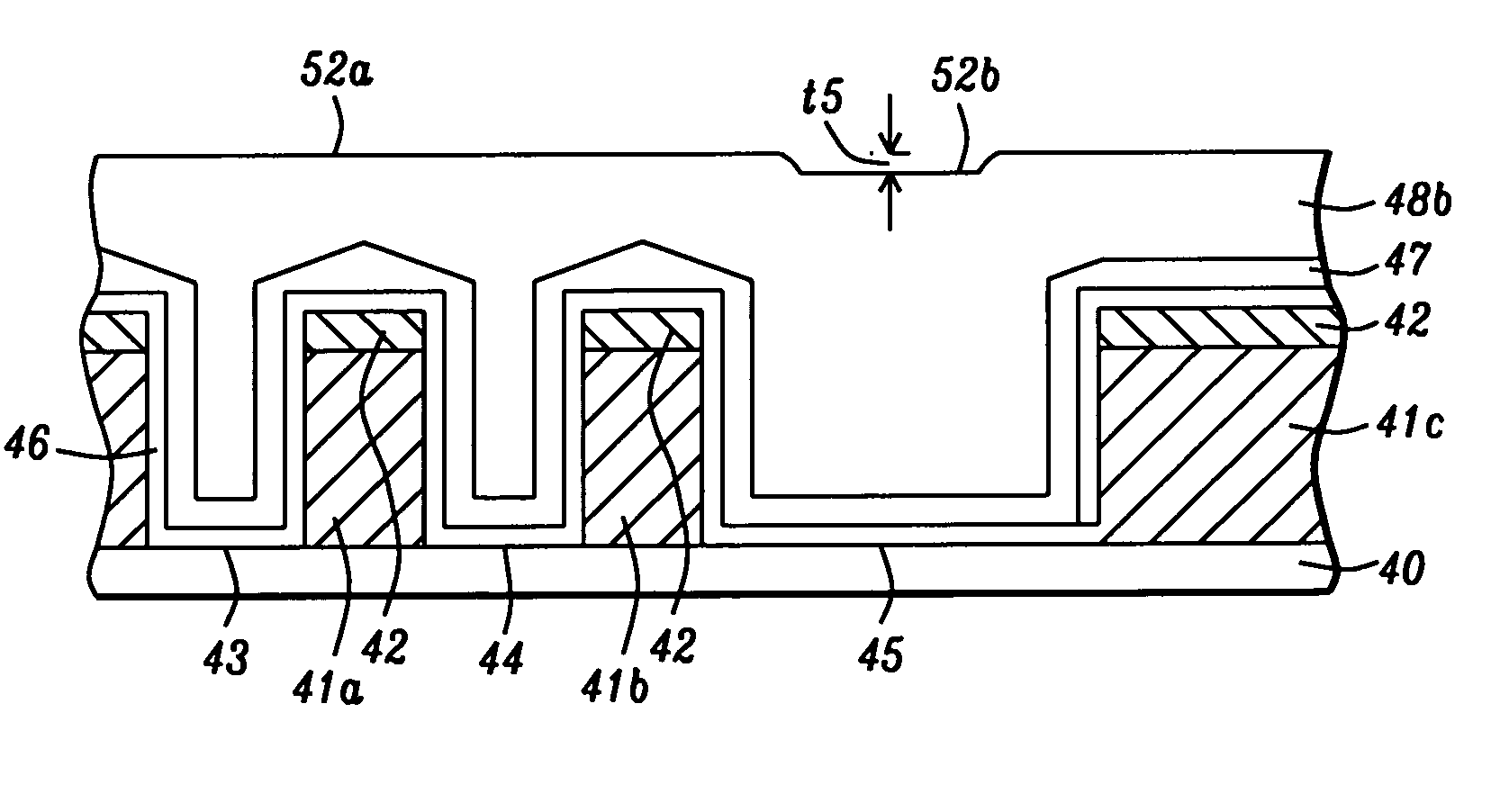
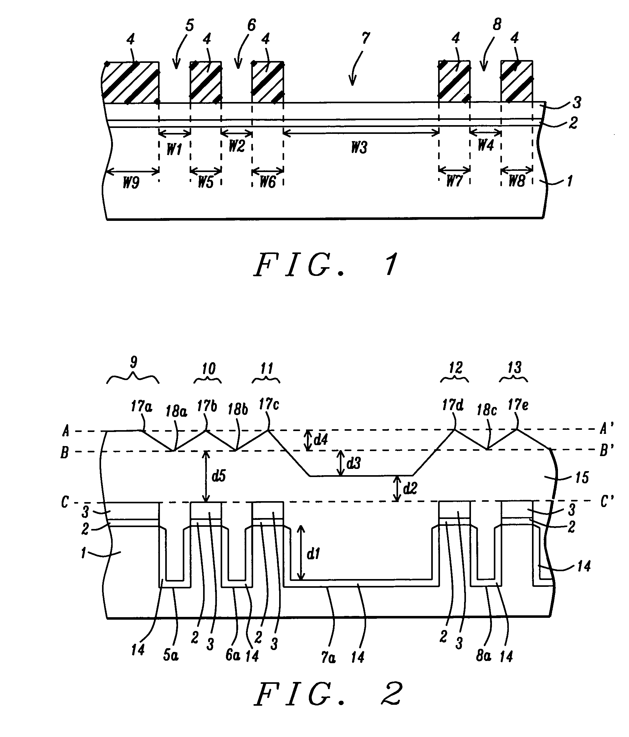
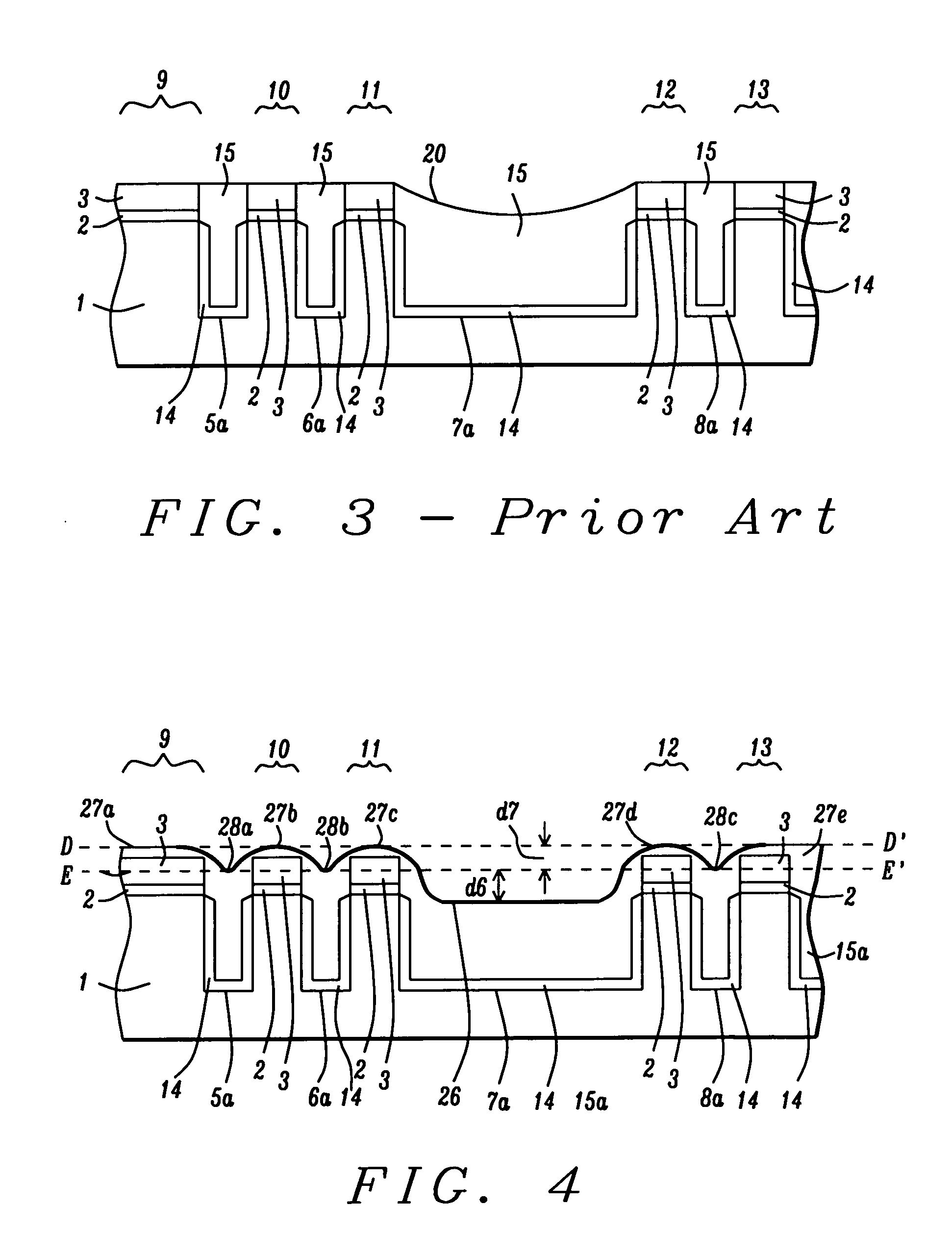
[0027] the present invention is depicted in FIGS. 1-2 and 4-7. Referring to FIG. 1, a substrate 1 is shown that is typically monocrystalline silicon but optionally may be based on a silicon-germanium, silicon-on-insulator, or other semiconductor materials used in the art. The substrate 1 generally contains a substructure (not shown) that includes active and passive devices. A pad oxide layer 2 with a thickness of about 50 to 200 Angstroms and preferably about 90 Angstroms is grown on the substrate 1 by an oxidation process that may be a rapid thermal oxidation (RTO), for example. Next, a chemical vapor deposition (CVD) technique or a diffusion thermal process is used to deposit a silicon nitride layer 3 having a thickness from between 600 and 1800 Angstroms and preferably about 800 to 1200 Angstroms on the pad oxide layer 2.

[0028] A commercially available photoresist is spin coated and baked on the silicon nitride layer 3 to give a photoresist layer 4 that is subsequently patterned ...


PUM


Abstract

A method of reducing oxide thickness variations in a STI pattern that includes both a dense trench array and a wide trench is described. A first HDP CVD step with a deposition / sputter (D / S) ratio of 9.5 is used to deposit a dielectric layer with a thickness that is 120 to 130% of the shallow trench depth. An etch back is performed in the same CVD chamber with NF3, SiF4 or NF3 and SiF4 to remove about 40 to 50% of the initial dielectric layer. A second HDP CVD step with a D / S ratio of 16 deposits an additional thickness of dielectric layer to a level that is slightly higher than after the first deposition. The etch back and second deposition form a smoother dielectric layer surface which enables a subsequent planarization step to provide filled STI features with a minimal amount of dishing in wide trenches.

Description

FIELD OF THE INVENTION [0001] The present invention relates to a method of fabricating an integrated circuit device, and in particular, to a method of forming shallow trench isolation (STI) features with a minimum amount of oxide thickness variation. BACKGROUND OF THE INVENTION [0002] As ground rules continue to shrink for devices in new technologies, device isolation regions called shallow trench isolation (STI) features have become increasingly popular as a means of separating active regions from one another. Devices such as transistors, resistors, and diodes are formed on active regions of a substrate. Increasing circuit density and improving device performance not only require that individual components of a device shrink in size but that the shallow trench isolation features are also reduced in dimension, especially the width or distance between adjacent active regions. [0003] Each pattern that is formed in a substrate is typically first printed in a photoresist layer by a lith...

Claims


Application Information

Patent Timeline
Patent Type & Authority Applications(United States)
IPC IPC(8): H01L21/3105H01L21/311H01L21/316H01L21/762
CPCH01L21/02164H01L21/02274H01L21/02304H01L21/76229H01L21/31055H01L21/31116H01L21/31612H01L21/31053
Inventor LU, CHIH-CHENGHOU, CHUAN-PINGFU, CHU-YUNWEN, CHANGMING, JANG SYUN
Owner TAIWAN SEMICON MFG CO LTD
Why Eureka
Try Eureka