

Photovoltaic conversion device and method of manufacturing the device
- Summary
- Abstract
- Description
- Claims
- Application Information
AI Technical Summary
Benefits of technology
Problems solved by technology
Method used
Image

Examples
example
[0187] An advantageous effect of the present invention will be described referring to a bulk multicrystalline silicon solar cell element fabricated according to the embodiment above.
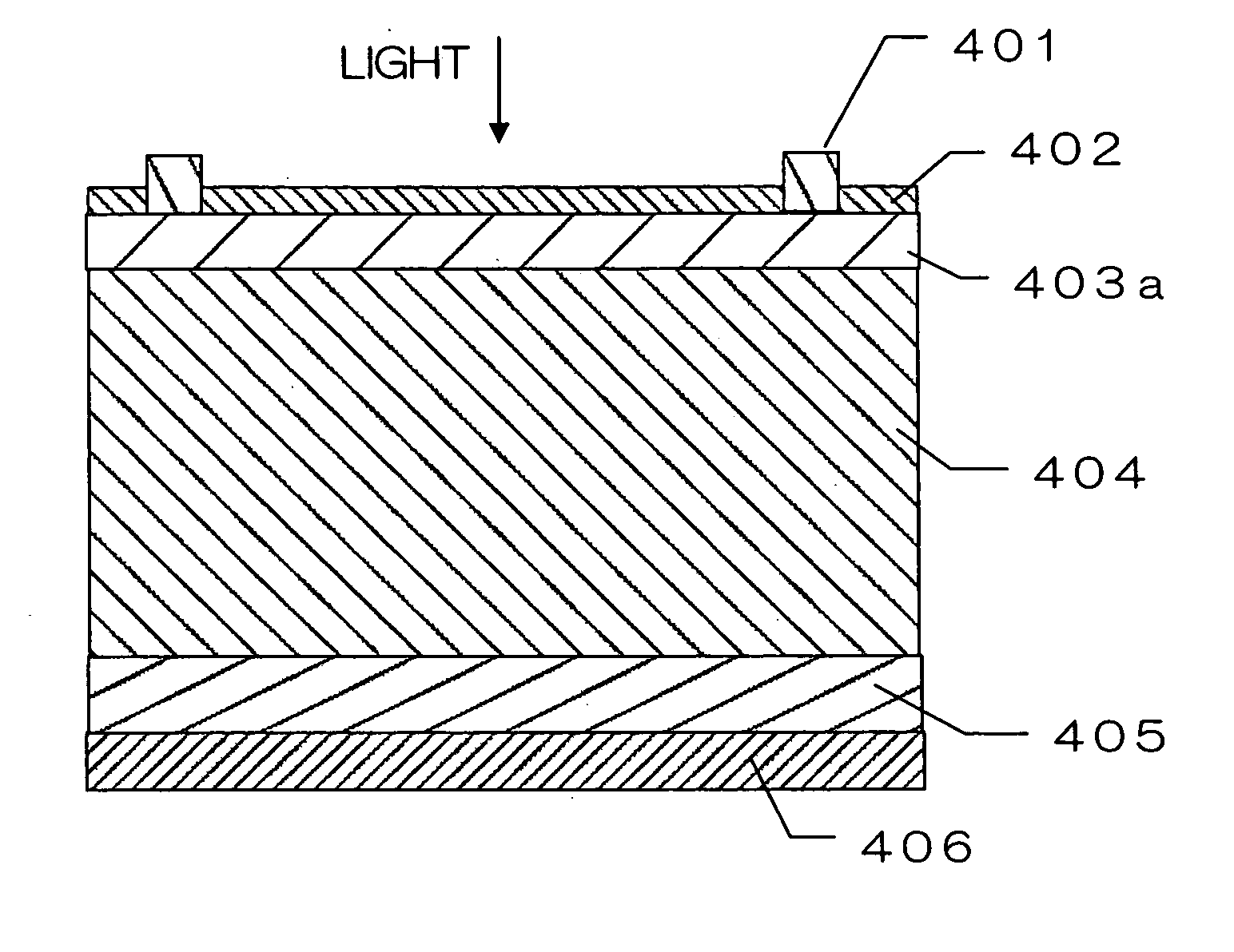
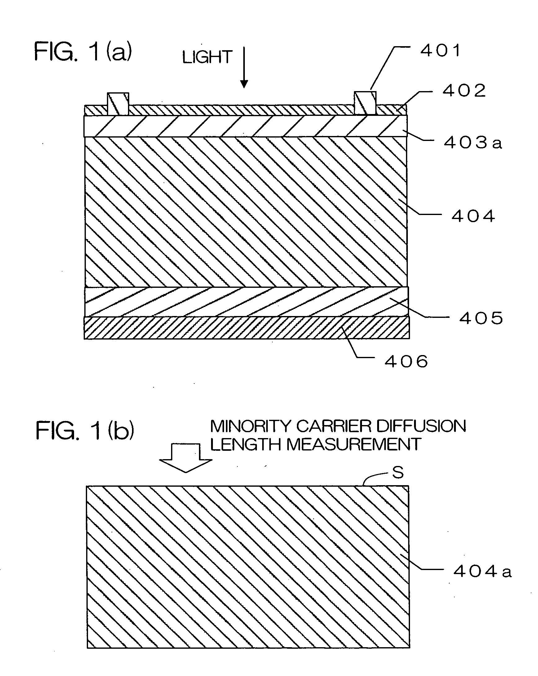
[0188] The substrate was-selected among multicrystalline silicon substrates produced by casting to be substrates shown in FIGS. 3 and 4 that have the low quality substrate peripheral regions originating from a side portion of the ingot with characteristic crystal grain configurations, which were used as the boron-doped p-type multicrystalline silicon substrate.
[0189] The dimensions of the substrate were 15 cm square and thickness thereof was 300 μm. [0190] 1) Minority carrier diffusion length of the substrate before processing for a solar cell element (before application of the present invention).
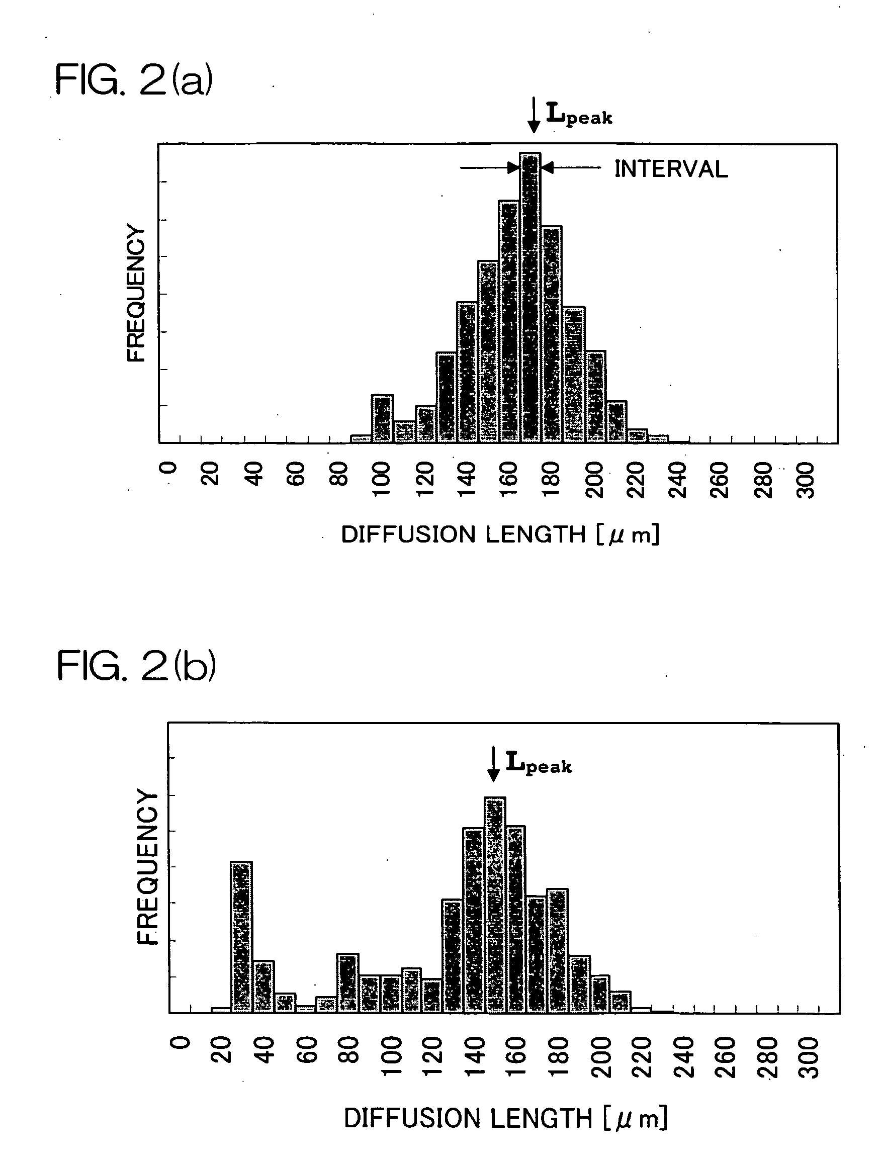
[0191] First, measurements of minority carrier diffusion lengths of these multicrystalline silicon substrates (before processing) were carried out. The measurement apparatus used was a SPV apparatus (Cat. No....
PUM
 Abstract
Description
Claims
Application Information