Mask blank manufacturing method and sputtering target for manufacturing the same

US20050170263A1Active Publication Date: 2005-08-04HOYA CORP
5 Cites 35 Cited by

Patent Information

Authority / Receiving Office
US · United States
Current Assignee / Owner
Publication Date
2005-08-04

Smart Images

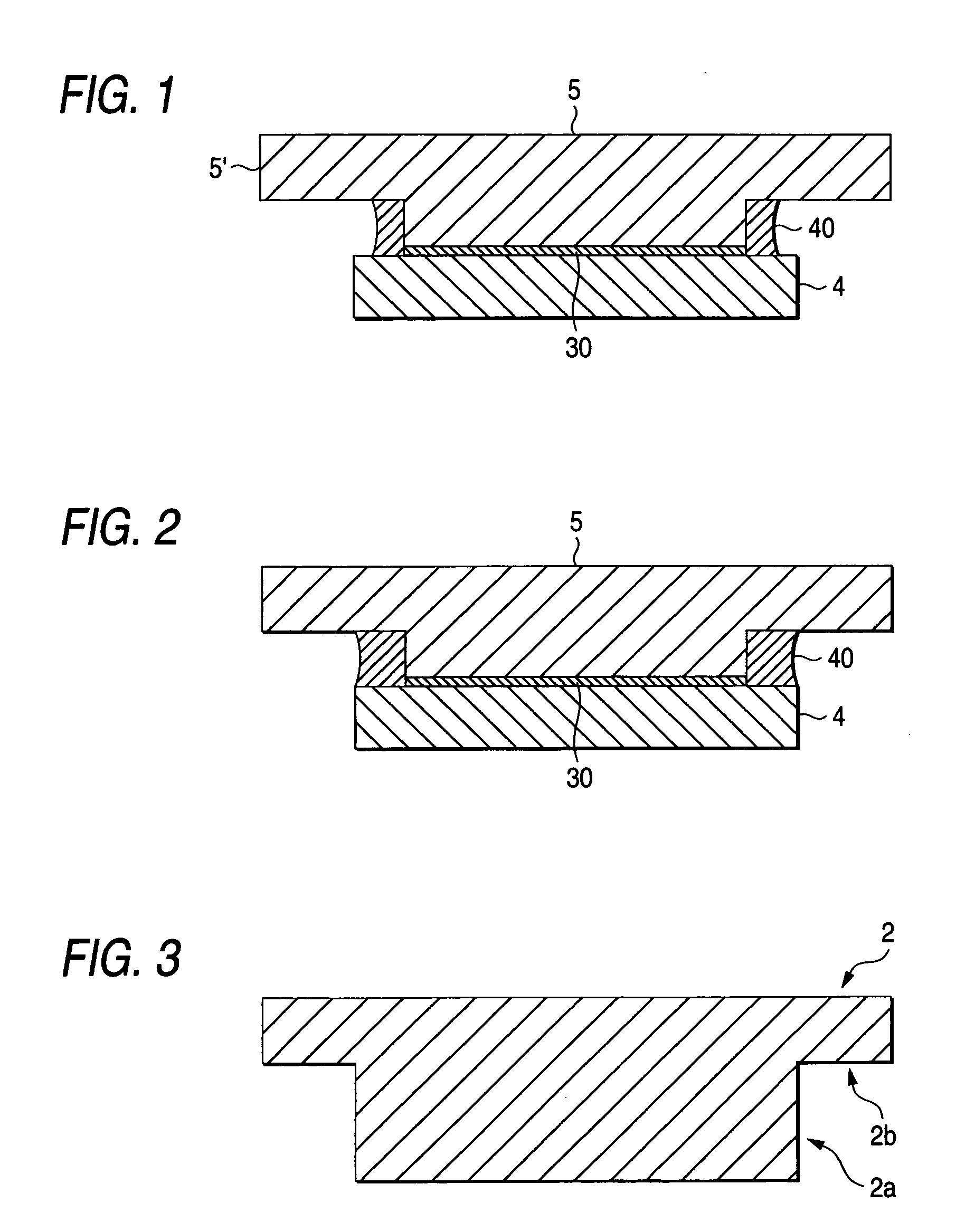
  • Figure 1
    Figure 1
  • Figure 2
    Figure 2
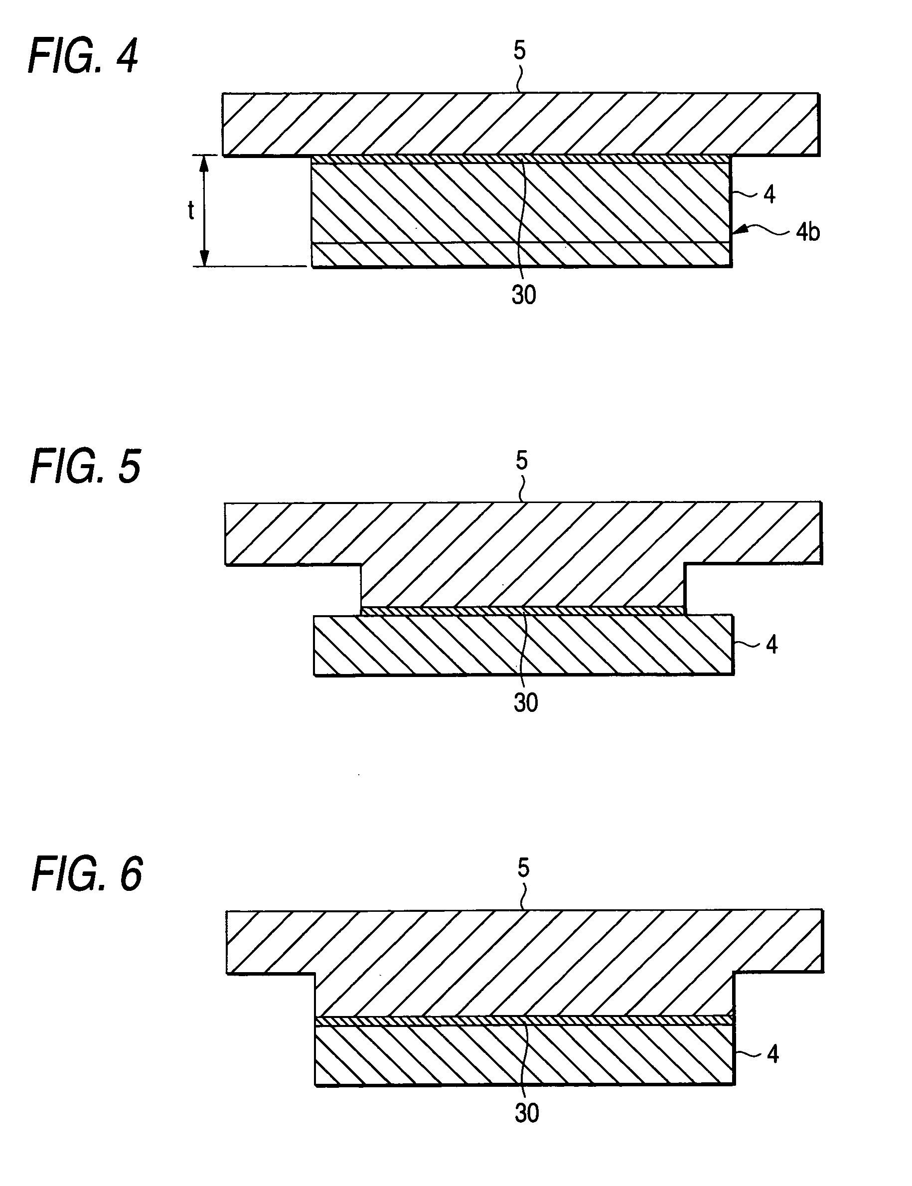
  • Figure 3
    Figure 3
Patent Text Reader

Abstract

A sputtering target for manufacturing a mask blank having a backing plate 5 where a portion for bonding a target member 4 is protruded like the convex with respect to a base portion 5′, and the target member 4 being formed to have a larger surface area than the area of the bonding portion of the backing plate 5 with extending from the bonding portion over a whole periphery with a bonding agent 30 interposed in-between, and further a metal 40 is deposited to a concave portion formed by a combination of the two structures in such a manner that the elution of the bonding agent 30 can be sealed.
Need to check novelty before this filing date? Find Prior Art

Description

[0001] This application claims priority based on Japanese Patent application No. 2004-002524, filed Jan. 7, 2004, the contents of which is incorporated herein by reference in its entirety. BACKGROUND OF THE INVENTION

[0002] 1. Field of the Invention

[0003] The present invention relates to a method of manufacturing a mask blank and a sputtering target for manufacturing a mask blank.

[0004] 2. Description of the Related Art

[0005] In recent years, a semiconductor device has been demanded to be processed more finely. For this reason, an exposure wavelength to be used has come to be shorter than before. With respect of such a short exposure wavelength, various technical requirements are demanded for realizing such a mask blank more severely.

[0006] For example, a light translucent film (a halftone phase shift film) in a phase shift mask blank of a halftone type is employed to meet the demanded requirements from both aspects of a light transmittance and a phase shift amount for an exposu...

Examples

example

[0090] An example of the invention will be described below in more detail.

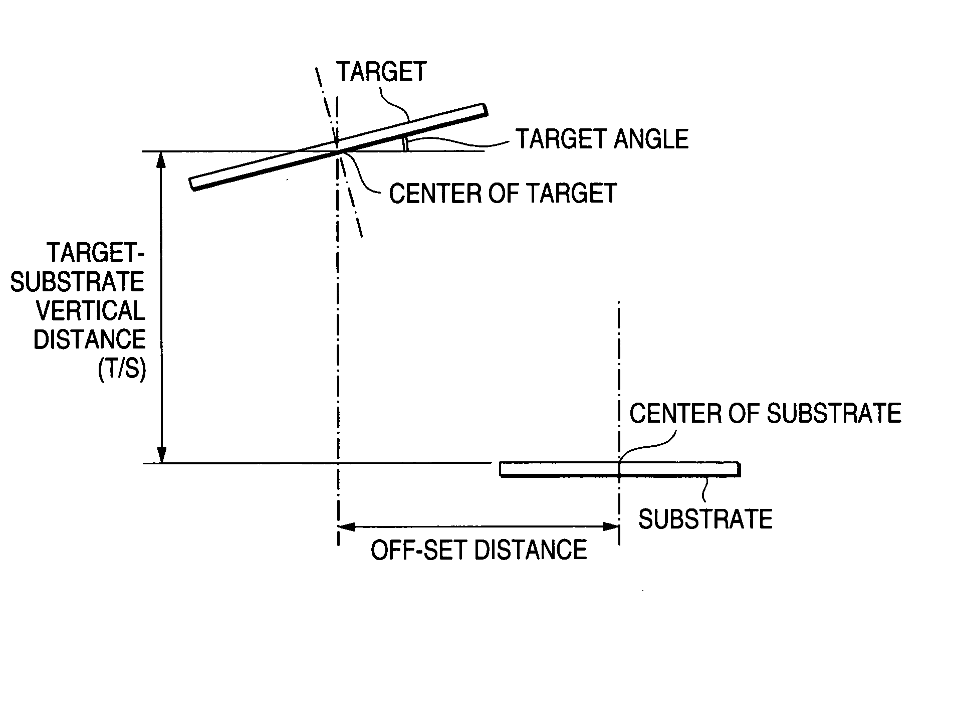
[0091] By using the DC magnetron sputtering apparatus described above with reference to FIGS. 7 to 9, 100 halftone contain phase shift mask blanks for an ArF excimer laser (193 nm) were fabricated one by one by continuously forming a film at a constant interval.

[0092] More specifically, a thin film (a thickness of approximately 670 angstroms) of molybdenum and silicon (MoSiN) nitrided on a transparent substrate (a quartz substrate of 6-inch square having a thickness of 0.25 inch) was formed through reactive sputtering (DC sputtering) in a mixed gas atmosphere (Ar: N2=10%:90%, a pressure: 0.1 Pa) of argon (Ar) and nitrogen (N2) by using a mixed target (Mo:Si=8:92 mol %) of molybdenum (Mo) and silicon (Si) so that a phase shift mask blank (a film composition of Mo:Si:N=7:45:48) for an ArF excimer laser (a wavelength of 193 nm) was obtained.

[0093] In the example, as shown in FIG. 7, there was used the apparatu...