Fabrication method of semiconductor device and semiconductor device
a technology of semiconductor devices and fabrication methods, which is applied in the direction of polycrystalline material growth, chemically reactive gases, crystal growth processes, etc., can solve the problems of increasing the fabrication cost of semiconductor devices, increasing the fabrication time of semiconductor devices, and forming speed of silicon-germanium films is relatively small, so as to improve the reliability and improve the fabrication yield.
- Summary
- Abstract
- Description
- Claims
- Application Information
AI Technical Summary
Benefits of technology
Problems solved by technology
Method used
Image
Examples
embodiment 1
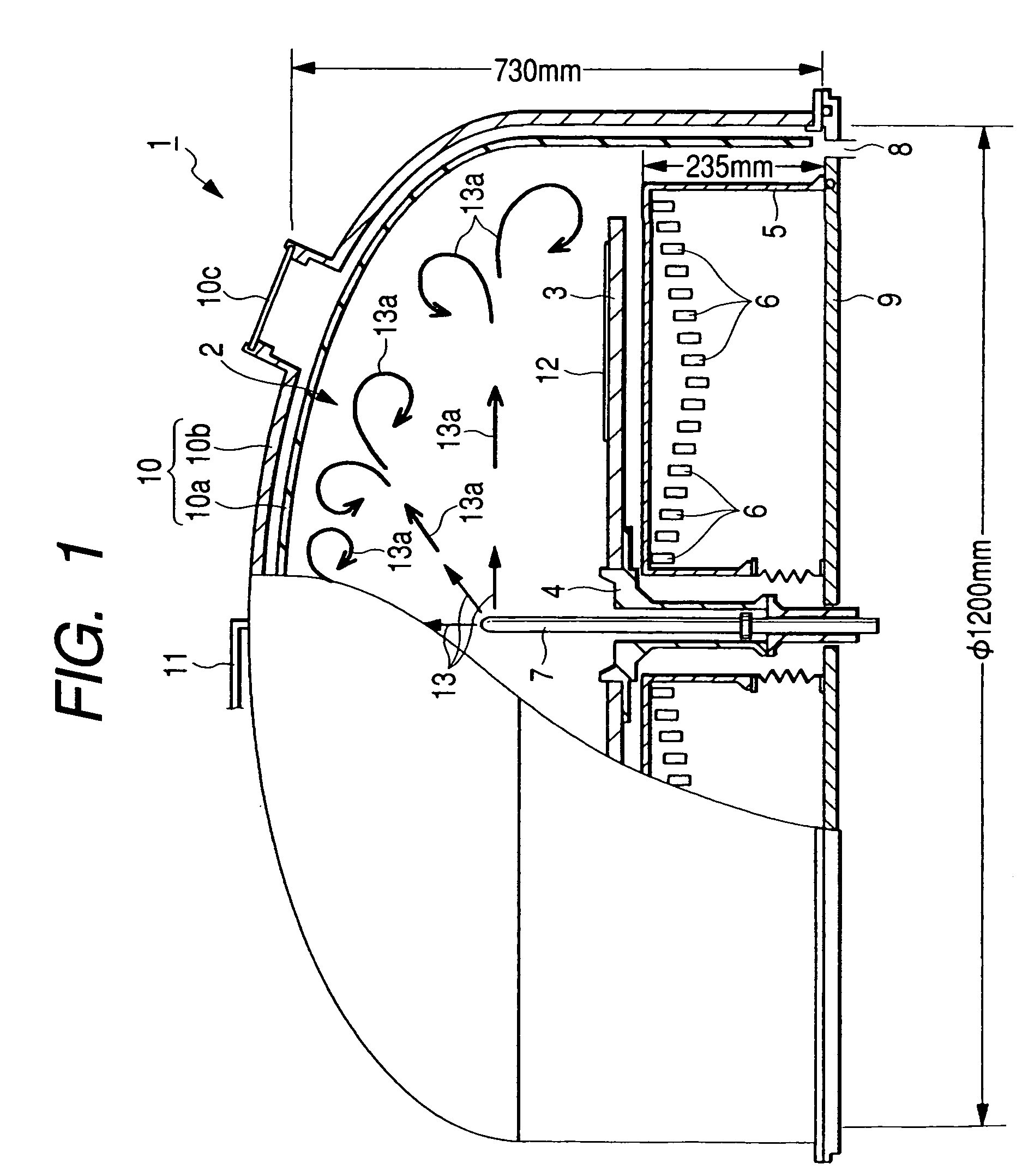
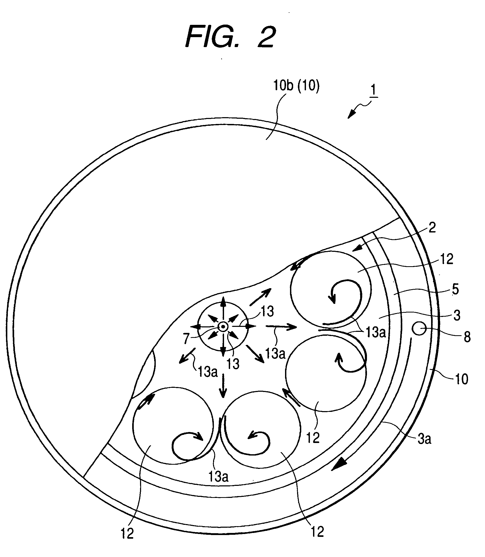
[0048]FIG. 1 is a front view, partially cut away, of a conceptional structure of a semiconductor fabricating apparatus used in the process of fabricating a semiconductor device according to this embodiment of the invention. FIG. 2 is a top view, partly cut away, of the semiconductor fabricating apparatus of FIG. 1. It will be noted that in FIG. 1, the cut away portion is shown as a conceptional section.
[0049] A semiconductor fabricating apparatus 1 shown in FIGS. 1 and 2 is a film-forming apparatus which is used in the process of forming a silicon-germanium film and a silicon film on a semiconductor substrate and is, for example, a batch-type CVD apparatus. It will be noted that for ease of understanding, structures other than a processing chamber and the inside thereof of the semiconductor fabricating device 1 are not particularly shown, with their detailed description being omitted.
[0050] The semiconductor fabricating apparatus 1 includes a reaction chamber or processing chamber...
embodiment 2
[0082]FIG. 10 is a view illustrating a semiconductor fabricating apparatus used in the process of fabricating a semiconductor device according to another embodiment of the invention.
[0083] A semiconductor fabricating apparatus 41 shown in FIG. 10 is a film-forming apparatus used in the process of forming a silicon-germanium film or a silicon film on a semiconductor substrate and is a single wafer processing CVD apparatus. For understanding in a simple way, the structure of the semiconductor fabricating apparatus 41 other than a processing chamber 42 and means or members provided in the inside thereof is not particularly shown with its detailed description being omitted.
[0084] The semiconductor fabricating apparatus 41 is provided with a processing chamber 42, a susceptor 43 arranged in the processing chamber 42, a susceptor support 44 for supporting the susceptor 43, a high frequency coil 46 disposed below the susceptor and accommodated in a coil cover 45, a gas nozzle 47 through ...
embodiment 3
[0093]FIG. 11 is a sectional view conceptionally showing the state wherein a silicon-germanium film 61 and a silicon film (strained silicon film) 62 are, respectively, formed on a semiconductor wafer (semiconductor substrate) 60.
[0094] The lattice constant of silicon-germanium increases with an increasing concentration of germanium. Accordingly, where the silicon-germanium film61 is formed on the semiconductor wafer 60 made of single crystal silicon, the epitaxial growth of a silicon-germanium film having a great concentration of germanium on the semiconductor wafer 60 incurs the possibility of causing inconveniences to occur in such a way that the silicon-germanium film is greatly strained owing the difference in lattice constant thereby causing defects of high density to be formed in the silicon-germanium film. To avoid this, the concentration of germanium in the silicon-germanium film 61 is made relatively small in the vicinity of the interface between the semiconductor wafer 60...
PUM
| Property | Measurement | Unit |
|---|---|---|
| pressure | aaaaa | aaaaa |
| pressure | aaaaa | aaaaa |
| pressure | aaaaa | aaaaa |
Abstract
Description
Claims
Application Information
 - R&D
- Intellectual Property
- Life Sciences
- Materials
- Tech Scout
- Unparalleled Data Quality
- Higher Quality Content
- 60% Fewer Hallucinations
Browse by: Latest US Patents, China's latest patents, Technical Efficacy Thesaurus, Application Domain, Technology Topic, Popular Technical Reports.
© 2025 PatSnap. All rights reserved.Legal|Privacy policy|Modern Slavery Act Transparency Statement|Sitemap|About US| Contact US: help@patsnap.com


