Normally off JFET

a technology of junction field effect transistor and jfet, which is applied in the direction of semiconductor devices, electrical equipment, transistors, etc., can solve the problem that jfet cannot be used for such applications

Active Publication Date: 2005-08-11
INFINEON TECH AMERICAS CORP
View PDF8 Cites 58 Cited by
  • Summary
  • Abstract
  • Description
  • Claims
  • Application Information

AI Technical Summary

Benefits of technology

[0006] In the present invention a plurality of limited area conduction channels are interposed in the current path from a source to a drain region. These conduction channels are defined between a gate region and a base region which are each of conductivity types opposite to that of the conduction or drift region, with a further island of the opposite conductivity type interposed between the base and gate regions. The chan

Problems solved by technology

However, JFETs are normally-on devices and are turned off by the application of a gate bias.
In many application circuits a nor

Method used


Image

  • Normally off JFET
  • Normally off JFET
  • Normally off JFET

Examples


Embodiment Construction

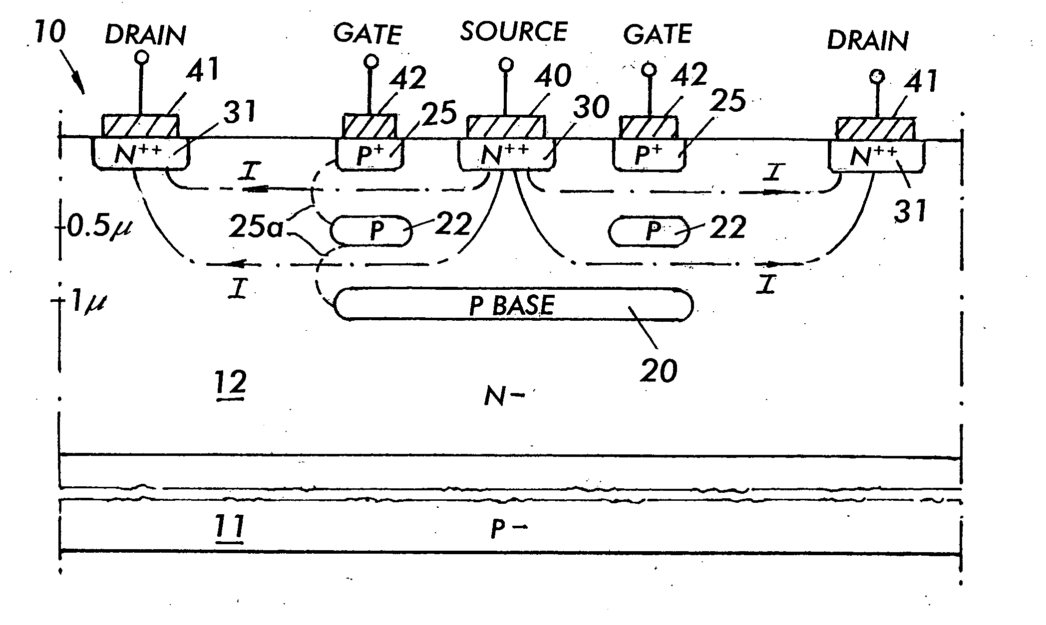
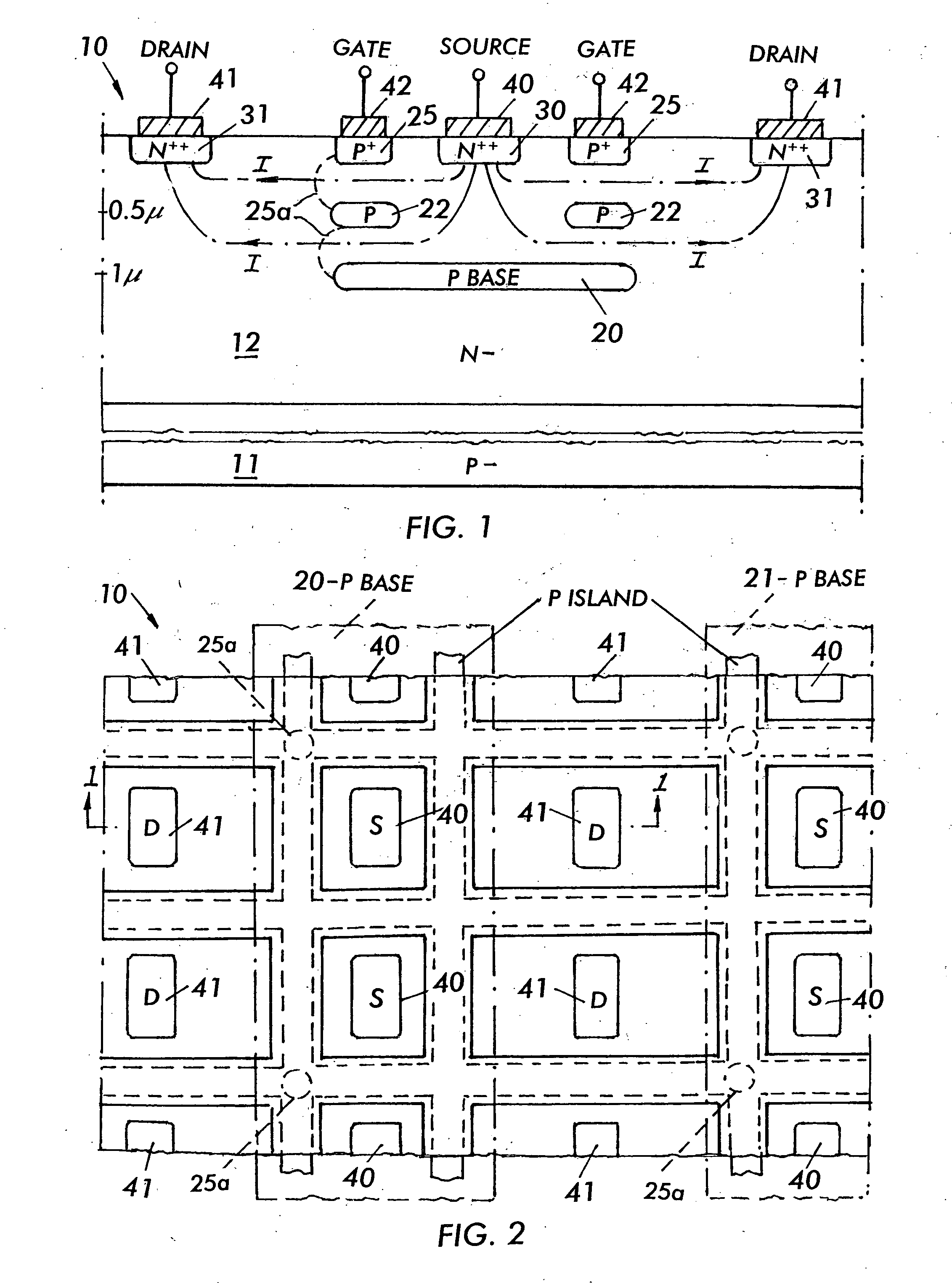
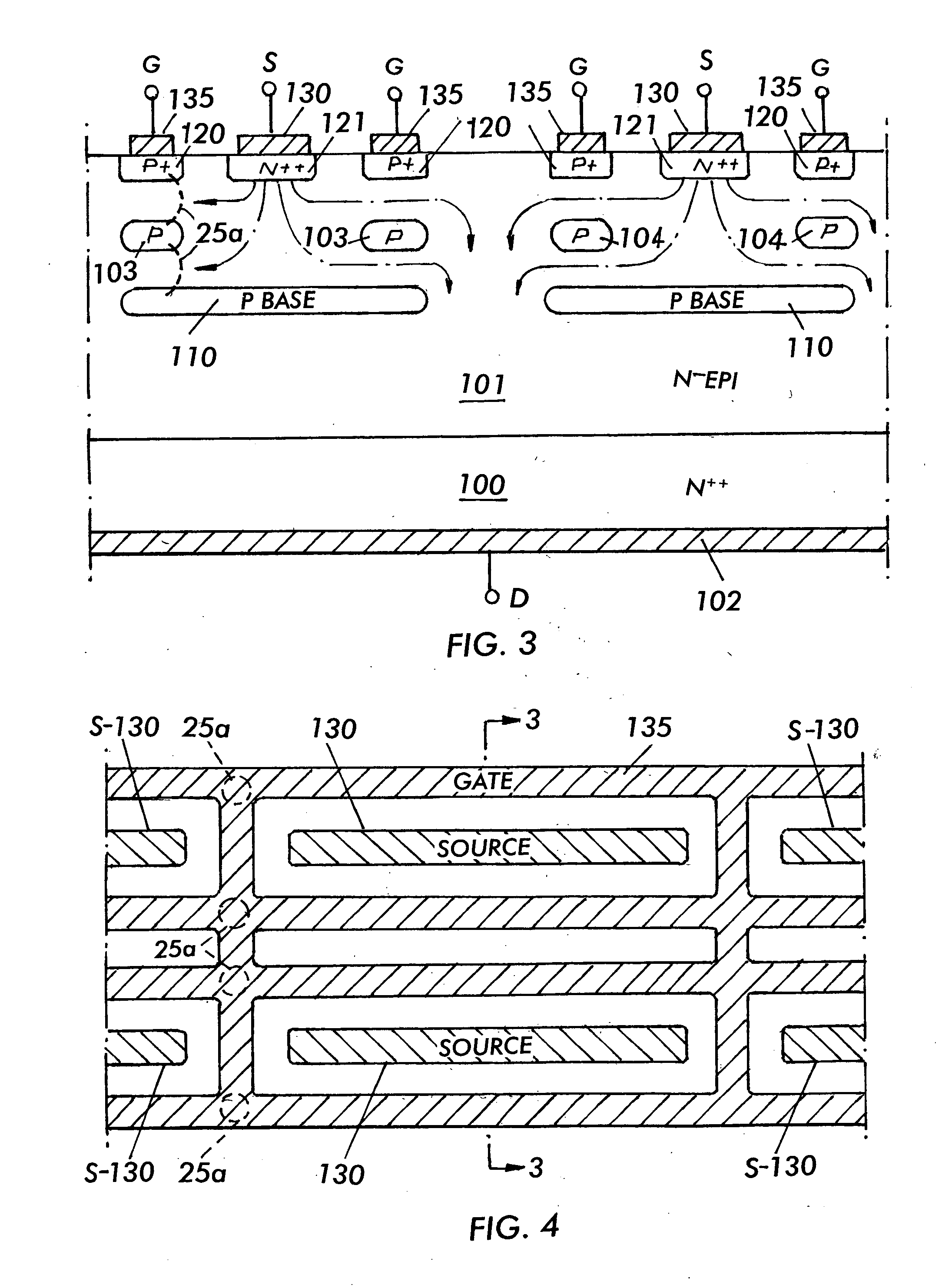
[0013] Referring first to FIGS. 1 and 2, there is shown a small portion of a wafer (or chip or die) 10 of silicon which has a P− substrate 11 which may have any desired thickness and which has an N− epitaxially deposited layer 12 thereon. Layer 12 may have a thickness of about 2.0 microns and a low impurity concentration, for example 1E16 / cm3.

[0014] A plurality of P bases 20 and 21 (FIG. 2) are implanted into the body of layer 12, and have a depth of about 1.0 micron and a thickness of about 0.05 microns. A P type grid or a P type “island” (in cross-section) 22 is next implanted to a depth of about 0.5 microns in the body of layer 12, and with a thickness of about 0.05 microns.

[0015] A P shallow gate contact implant 25 is then implanted into the top of layer 12 and aligned to the grid 22; and N++ source and drain contact regions 30 and 31 respectively are also implanted into the top surface of region 12. Aluminum source contacts 40 are then formed atop region 30; aluminum drain co...


PUM


Abstract

A normally off JFET is formed by the implantation of a P base; and a shallower P island atop the P base, forming a narrow lateral conduction channel between the two and a shallow gate implant in the device top surface which forms a second lateral conduction channel with the island. The two channels are each less than 0.5 microns thick and have an impurity concentration such that the channels are depleted at zero gate voltage and are turned on when the gate is forward biased. The gate surrounds a source implant region and a remote drain is provided which is connected to the top surface of the device for a lateral JFET or the bottom of the device for a vertical conduction JFET.

Description

RELATED APPLICATION [0001] This application claims the benefit of U.S. Provisional Application No. 60 / 543,163, filed Feb. 9, 2004FIELD OF THE INVENTION [0002] This invention relates to semiconductor devices and more specifically relates to a junction field effect transistor (JFET) which is normally off. BACKGROUND OF THE INVENTION [0003] JFETs are well known transistors having numerous desirable characteristics. However, JFETs are normally-on devices and are turned off by the application of a gate bias. In many application circuits a normally-off transistor is needed so that the JFET cannot be used for such applications without additional gate control circuits. [0004] It would be very desirable to provide a JFET which is normally-off; that is, non-conductive in the absence of the presence of a gate turn off signal, and which is turned on by the presence of a gate signal. BRIEF DESCRIPTION OF THE INVENTION [0005] In accordance with the present invention, a novel JFET is provided whic...

Claims


Application Information

Patent Timeline
IPC IPC(8): H01L29/06H01L29/423H01L29/808
CPCH01L29/0692H01L29/8083H01L29/808
Inventor POTTS, ALAN
Owner INFINEON TECH AMERICAS CORP
Why Eureka
Try Eureka