Image sensor and method of manufacturing the same

a technology of image sensor and manufacturing method, which is applied in the field of image sensor, can solve the problems the low power consumption the limitation of reducing the size of the pixel array, so as to achieve the effect of easy expansion of the area occupied by the photodiod

Active Publication Date: 2005-08-11
INTELLECTUAL VENTURES II
View PDF13 Cites 20 Cited by
  • Summary
  • Abstract
  • Description
  • Claims
  • Application Information

AI Technical Summary

Benefits of technology

[0013] With the present invention, all or a portion of the metal wiring consisting of the lower metal wiring, the plug, and the upper metal wiring is formed in a transparent conductive film pattern. As such, the metal wiring can be formed on the photodiode, so that the area occupied by the photodiode can be easily enlarged. That is, the metal wiring of the transparent conductive film pattern is employed, which does not impede transfer of light to the photodiode.

Problems solved by technology

In addition, the CMOS image sensor is inexpensive and consumes a low power, because of utilizing a compatible CMOS technique.
In the case of securing the occupied region, there is a problem in that the pixel array is largely sized.
In addition, since the region occupied by the pixel array is determined after a peripheral cell region is secured, there is a limitation of reducing a size of the pixel array.
Such as, a conventional CMOS image sensor has some advantages, but it is difficult to enlarge an area to be occupied by the photodiode, which may not obtain an image of high resolution.

Method used


Image

  • Image sensor and method of manufacturing the same
  • Image sensor and method of manufacturing the same
  • Image sensor and method of manufacturing the same

Examples


Embodiment Construction

[0018] Hereinafter, a preferred embodiment of the present invention will be described with reference to the accompanying drawings. In the following description and drawings, the same reference numerals are used to designate the same or similar components, and so repetition of the description on the same or similar components will be omitted.

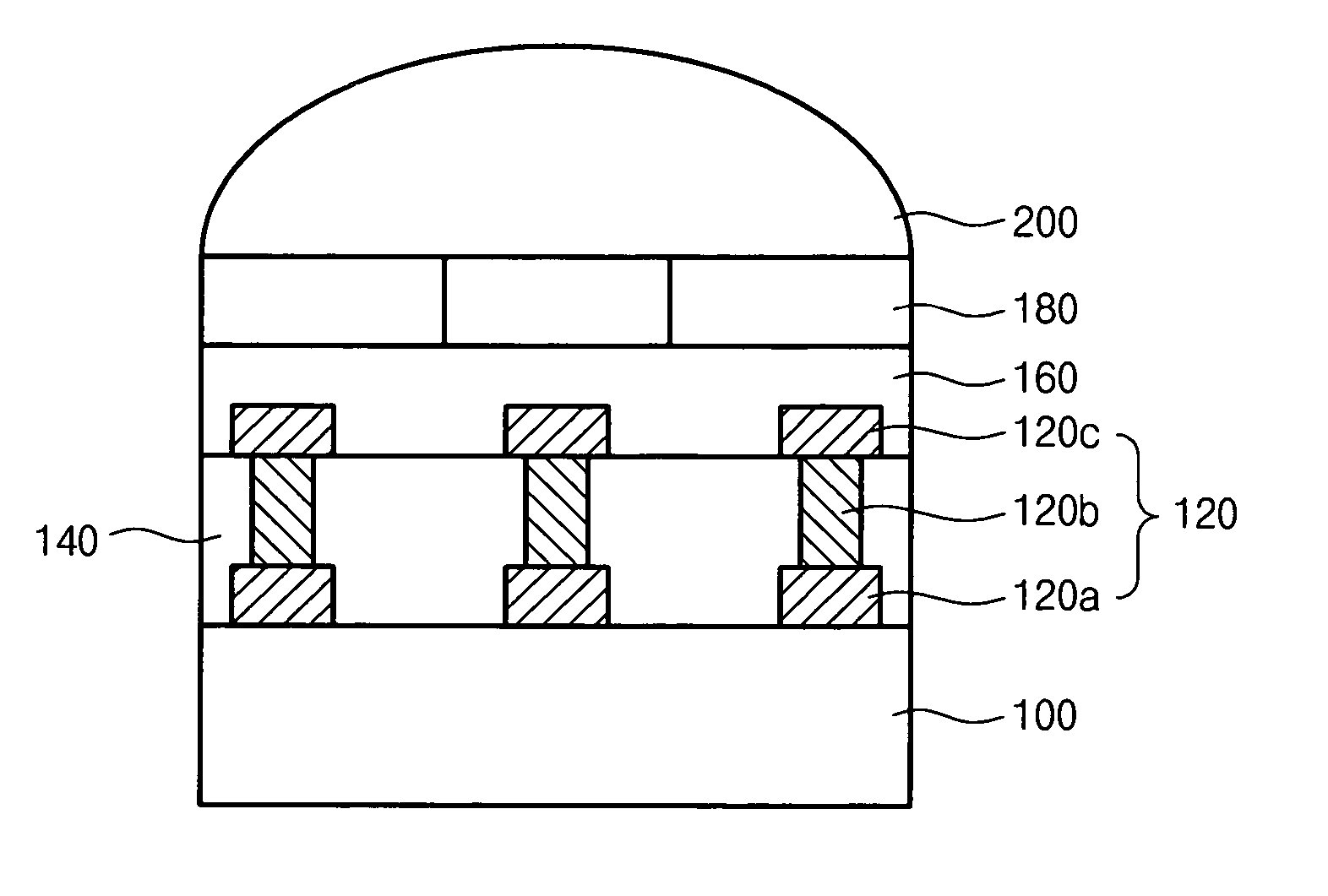
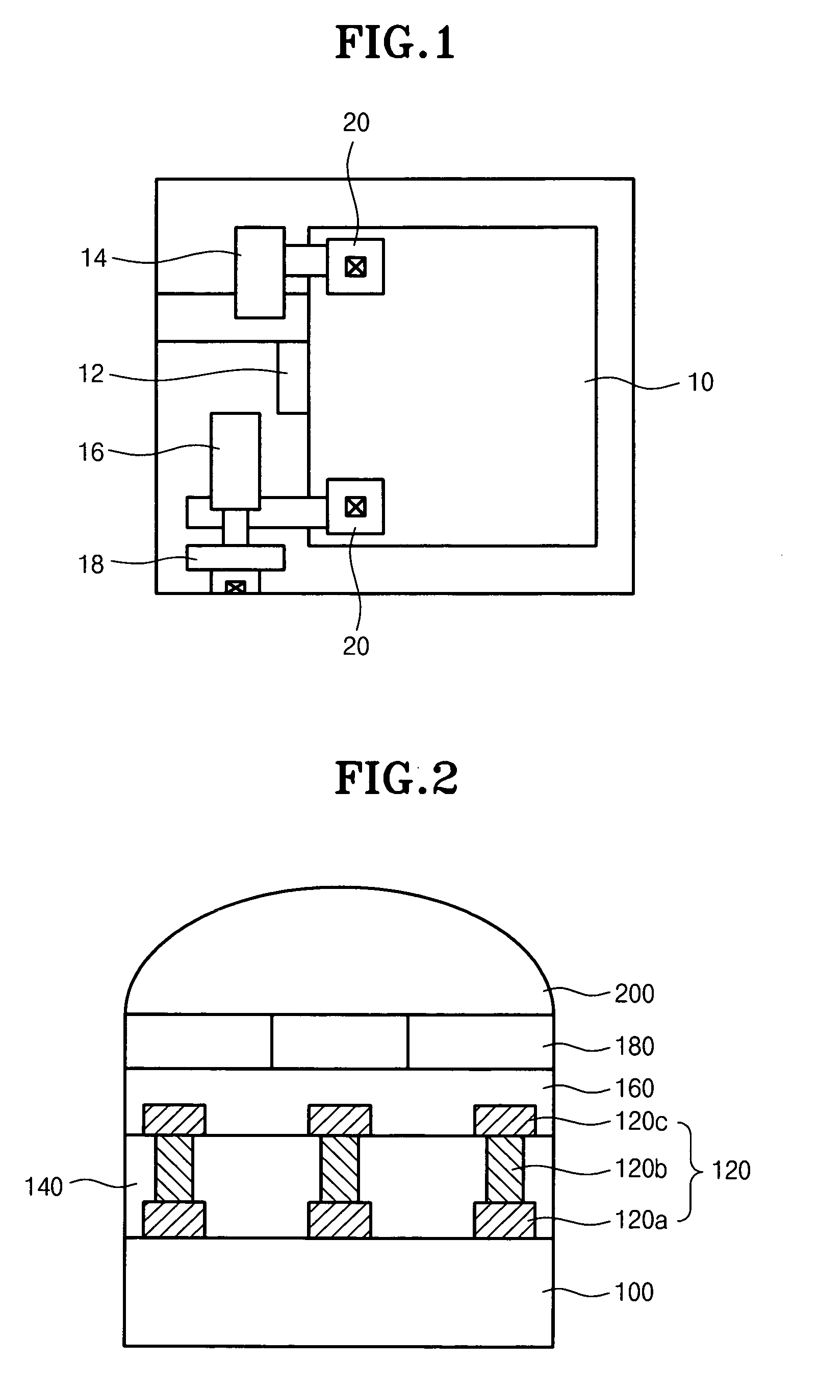
[0019]FIG. 1 is a schematic view depicting a layout of a pixel array of an image sensor according to a preferred embodiment of the present invention.

[0020] Referring to FIG. 1, a pixel diode includes a photodiode 10 for detecting light and four transistors, which form a unit pixel. Among four transistors, a transfer transistor 12 is to transfer a charge stored in the photodiode to a floating diffusion region, a reset transistor 14 is to reset the floating diffusion region as a supply voltage level, a drive transistor 16 serves as a source follower, and a selection transistor 18 is to receive a pixel data enable signal and output a pixel data si...


PUM

PropertyMeasurementUnit
pressureaaaaaaaaaa
temperatureaaaaaaaaaa
transparent conductiveaaaaaaaaaa

Abstract

Disclosed are an image sensor and a method of manufacturing the same. A metal wiring consisting of a lower metal wiring, an upper metal wiring, and a plug connecting the lower and upper metal wirings, in which the lower and upper metal wiring are made of a transparent conductive film pattern, is formed on a substrate with devices formed thereon, the devices including a photodiode and gate electrodes. Then, a passivation film, a color filter, and a microlens are sequentially formed on the metal wiring. All or a portion of the metal wiring is formed in a transparent conductive film pattern. As such, the metal wiring is formed on the photodiode.

Description

BACKGROUND OF THE INVENTION [0001] 1. Field of the Invention [0002] The present invention relates to a device for converting photons into charge packets, and more particularly to an image sensor with a metal wiring and a method of manufacturing the image sensor. [0003] 2. Description of the Prior Art [0004] An image sensor is a device for converting one or two-dimensional optical image into an electrical signal. The image sensor is a kind of a solid-state image sensor which is generally divided into a CMOS (Complementary Metal Oxide Semiconductor) image sensor and a CCD (Charge Coupled Device) image sensor. [0005] The CMOS image sensor converts an optical image into an electrical signal, and employs a switch mode to detect outputs one by one using MOS transistors which are made as many as the number of pixels by use of CMOS manufacturing technique. In particular, the CMOS image sensor has advantages in that a driving mode is simple, various scanning modes can be embodied, and a sign...

Claims


Application Information

Patent Timeline
Patent Type & Authority Applications(United States)
IPC IPC(8): H01L27/148H01L27/14H01L27/146H01L31/10H01L31/18
CPCH01L27/14601H01L27/14632Y02E10/50H01L27/14687H01L31/1884H01L27/14636H01L27/148H01L31/10
Inventor KIM, HEE JEEN
Owner INTELLECTUAL VENTURES II
Why Eureka
Try Eureka