Delay signal generation device and recording pulse generation device

a signal generation device and delay signal technology, applied in the direction of pulse technique, single output arrangement, instruments, etc., can solve the problems that the circuit scale of the write strategy circuit the circuit scale of the recording controller cannot be substantially increased, so as to achieve the effect of suppressing the increase in the circuit scal

Inactive Publication Date: 2005-08-11
SEMICON COMPONENTS IND LLC
View PDF6 Cites 11 Cited by
  • Summary
  • Abstract
  • Description
  • Claims
  • Application Information

AI Technical Summary

Benefits of technology

[0007] Accordingly, it is an object of the present invention to provide a delay signal generator and a recording pulse generator that optimally suppress an increase in their circuit scales even when generating, for a single input signal, a plurality of delay signals differing from one another in the minimum unit of delay amounts.

Problems solved by technology

However, such recording controllers and reproduction controllers cannot be constructed without a substantial increase in their circuit scale.
This inevitably enlarges the circuit scale of the write strategy circuit.
The above-described problem is not limited to the write strategy circuit, but commonly occurs with any delay signal generator that generates, from a single input signal, a plurality of delay signals differing from one another in the minimum unit of delay amount.

Method used


Image

  • Delay signal generation device and recording pulse generation device
  • Delay signal generation device and recording pulse generation device
  • Delay signal generation device and recording pulse generation device

Examples


Embodiment Construction

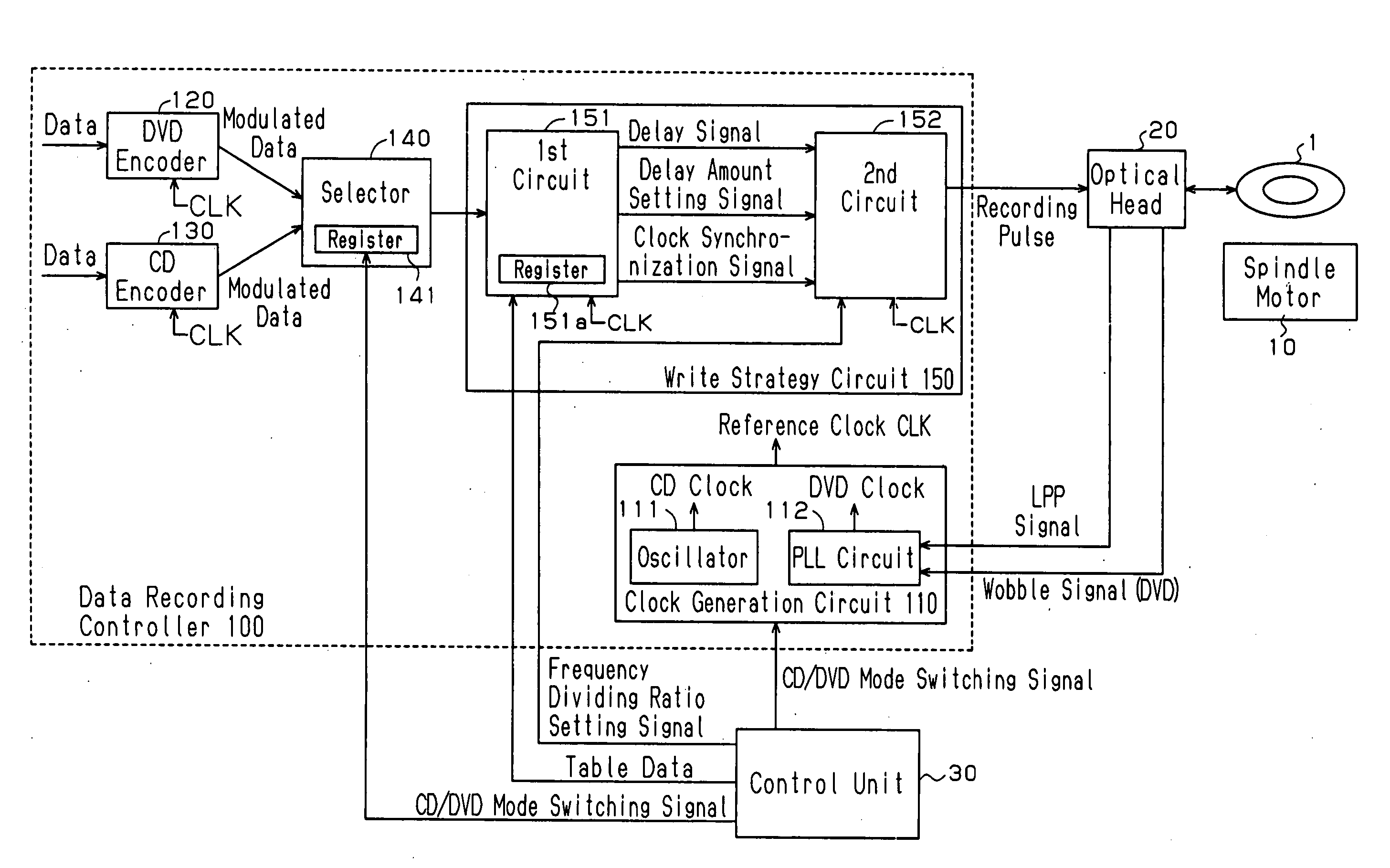
[0015] A recording pulse generator according to a preferred embodiment of the present invention applied to a write strategy circuit for CDs and DVDs will now be described with reference to the drawings.

[0016]FIG. 1 is a block diagram showing the configuration of a data recording controller, including the write strategy circuit, and its peripheral circuits.

[0017] In FIG. 1, an optical disc 1, which is controlled to be rotated with a constant linear velocity by a spindle motor 10, is a CD (CD-R or CD-RW) or a DVD (DVD-R or DVD-RW). On the optical disc 1, regardless of whether it is a CD or a DVD, a single spiral track is formed as a data recording area. The track is formed by creating a groove in a flat surface (land) of the disc.

[0018] When the optical disc 1 is a CD, the groove is slightly wobbled. Information called ATIP (Absolute Time In Pregroove) is recorded where a cycle change occurs in the wobble of the groove. By tracing the track to read the ATIP information written in t...


PUM

PropertyMeasurementUnit
frequencyaaaaaaaaaa
frequency dividing ratioaaaaaaaaaa
phaseaaaaaaaaaa

Abstract

A write strategy circuit (recording pulse generator) generates a recording pulse for controlling a laser output applied to an optical disc using data modulated by a DVD encoder or a CD encoder. A delay circuit (220) delays delay subject signals S1 to S4 by a predetermined amount to generate delay signals D1 to D4. A delay amount for the delay circuit (220) is controlled by a delay amount control circuit (210). A logic circuit (300) generates a recording pulse by logically synthesizing the delay signals D1 to D4. The delay amount control circuit includes a voltage controlled oscillator formed by connecting, in a ring-like manner, a plurality of delay elements (211a) having the same configuration as the delay elements (221) included in the delay circuit. An output signal of the voltage controlled oscillator is locked at a point where a delay amount for each delay element (211a) becomes a fraction of an integer of one cycle of a reference clock signal.

Description

TECHNICAL FIELD [0001] The present invention relates to a delay signal generator that is capable of generating, for a single input signal, a plurality of differing delay signals having different minimum units of delay amounts, and to a recording pulse generator that is capable of retrieving modulated data, which has been subjected to predetermined modulation, and generating recording pulses for at least two different disc media. BACKGROUND ART [0002] A data recorder, which records desired data using a laser on a disc medium functioning as a recording medium, such as an optical disc, usually includes a write strategy circuit. The write strategy circuit generates a timing signal for controlling the state of laser irradiation. One example of such a timing signal is a recording pulse, which is generated by pulse-modulating data subject to recording, for controlling the intensity and time of laser irradiation on a disc medium. The laser irradiation is carried out according to the recordi...

Claims


Application Information

Patent Timeline
Patent Type & Authority Applications(United States)
IPC IPC(8): G11B20/10G11B7/0045G11B7/006G11B7/125G11B7/126G11B20/14H03K5/00H03K5/13H03L7/08H03L7/081H03L7/099H03L7/18H04L7/033
CPCG11B7/00456G11B7/0062G11B7/126G11B20/10H04L7/0337H03K2005/00039H03L7/0805H03L7/0995H03L7/18H03K5/133G11B7/0045H03L7/00H04L7/033
Inventor SHUTOKU, TOSHIYUKITOMISAWA, SHIN-ICHIRO
Owner SEMICON COMPONENTS IND LLC
Why Eureka
Try Eureka