Semiconductor device and its manufacturing method

a semiconductor device and manufacturing method technology, applied in semiconductor devices, semiconductor/solid-state device details, electrical equipment, etc., can solve the problems of increasing the number of external terminals, and increasing the package size, so as to reduce the thickness of the semiconductor device, reduce the size of the sealing member, and reduce the size

Inactive Publication Date: 2005-08-11
RENESAS ELECTRONICS CORP
View PDF13 Cites 33 Cited by
  • Summary
  • Abstract
  • Description
  • Claims
  • Application Information

AI Technical Summary

Benefits of technology

[0035] (d) Conductors are provided on terminal surfaces exposed to the back surface of the insulating resin layer to form salient electrodes, thus affording a so-called stand-off structure. Therefore, even if fine dust particles are present on a packaging substrate at the time of packaging the semiconductor device, it is possible to effect packaging without any trouble.
[0036] According to the above means (3), since product forming portions are provided in a matrix form on the tape and, after the insulating resin layer is formed, the same layer is cut longitudinally and transversely to fabricate semiconductor devices, it is possible to decrease the size of the sealing member formed by the insulating resin layer and a large number of small-sized and thin semiconductor devices can be manufactured at a time.
[0037] According to the above means (4), it is possible to fabricate a semiconductor device with a semiconductor element fixed onto a semiconductor element fixing piece(s) formed using the same material as the material of the terminals on the main surface of the tape. With this construction, the back surface of the semiconductor element is protected and therefore the semiconductor element can be made thinner, thus permitting the reduction in thickness of the semiconductor device.
[0038] According to the above means (5), the back surface of the semiconductor element is not directly exposed to the back surface of the sealing member formed by the insulating resin layer, but the back surface of the semiconductor element is covered with an insulating adhesive. Thus, an electric insulation on the back side of the semiconductor element can be ensured.
[0039] According to the above means (6), since terminals are arranged in a matrix form on the back surface of the sealing member formed by the insulating resin layer, the semiconductor device fabricated has a larger number of external electrode terminals (pins) in a smaller area. Thus, it is possible to attain the reduction in size and an increase in the number of pins of the semiconductor device.
[0040] According to the above means (7), the terminals are positioned inside the outer periphery edges of the insulating resin layer, so even if the semiconductor device is mounted in proximity of another electronic part such as another semiconductor device, no short-circuit occurs between it and the electronic part adjacent thereto and hence the packaging reliability is improved.

Problems solved by technology

In a non-leaded semiconductor device, a lead surface exposed to one side of a package serves as a packaging surface and therefore the packaging area is small in comparison with such a semiconductor device as SOP (Small Outline Package) or QFP wherein leads are projected from side faces of a package, but since external terminals are arranged in one row along an outer periphery of a semiconductor chip, an increase in size of the package is unavoidable with an increase in the number of external terminals, thus giving rise to the problem that such an increase of the package size is unsuitable for constructing a semiconductor device having a larger number of pins.
However, forming such a construction by utilizing a lead frame leads to an increase of cost.
Thus, it is difficult to reduce the material cost.
Forming a thick metallic plate into a desired pattern with a high accuracy by selective etching or using a precision press is difficult as noted above.
In addition, disposing formed external terminal parts onto a resin film requires much time and labor, as described in Japanese Unexamined Patent Publication No. 2000-77596.
On the other hand, in the case of TBGA fabricated using an insulating tape, the tape cost is high, thus obstructing the attainment of reducing the cost of the semiconductor device.
Thus, the use of an expensive material is unavoidable, which is a cause of an increase of cost.
Thus, also in point of structure, the tape cost becomes high.

Method used


Image

  • Semiconductor device and its manufacturing method
  • Semiconductor device and its manufacturing method
  • Semiconductor device and its manufacturing method

Examples


first embodiment

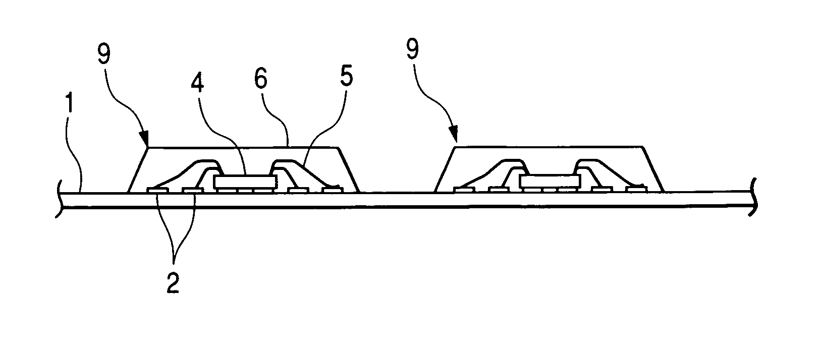
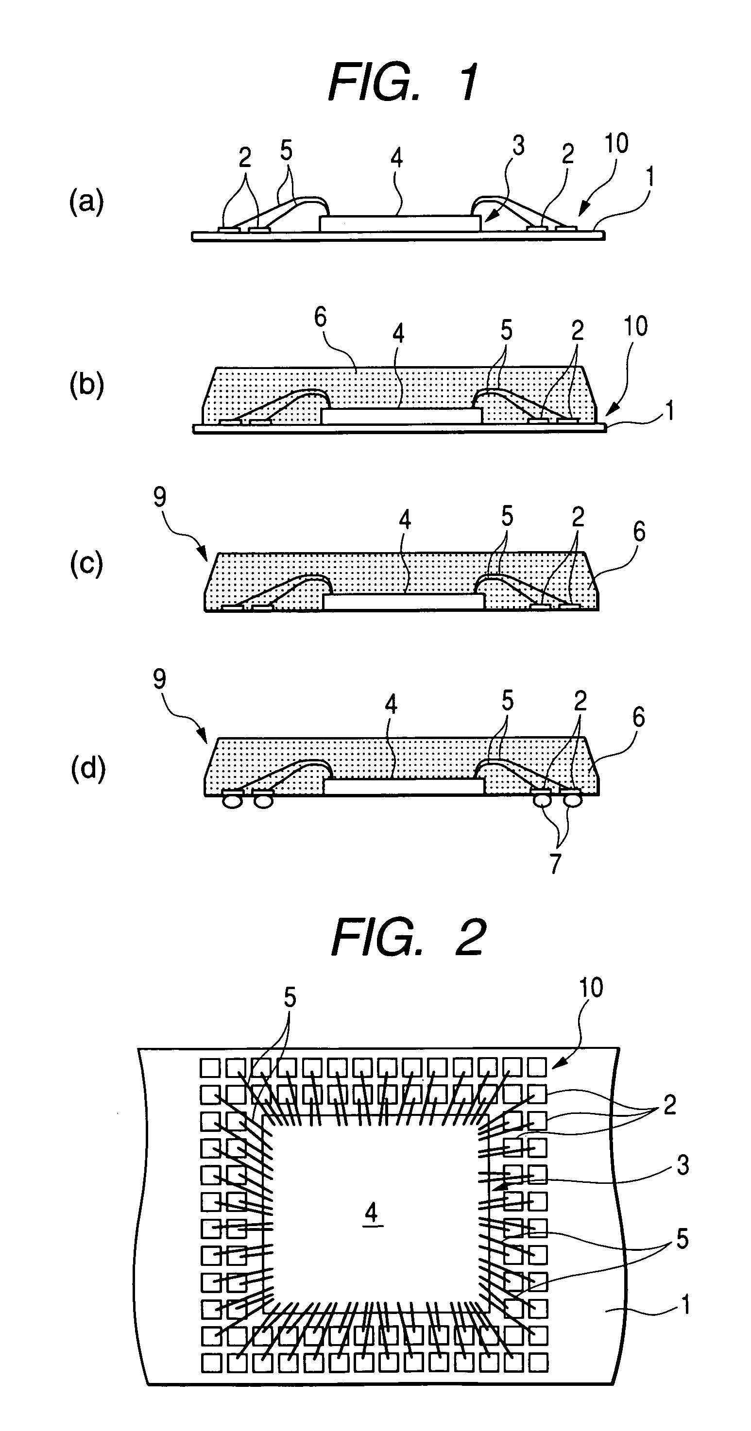
[0093] FIGS. 1 to 6 illustrate a method of manufacturing a non-leaded, resin-sealed type semiconductor device according to an embodiment (first embodiment) of the present invention. In this first embodiment, such a semiconductor device as shown in FIG. 1(d) is fabricated through such steps as shown in FIGS. 1(a) to 1(d).

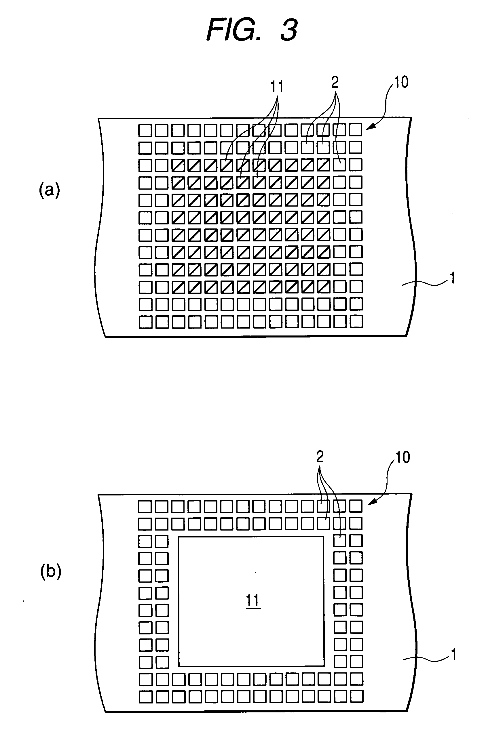
[0094] First, as shown in FIG. 1(a), a flexible tape 1 is provided. Plural terminals 2 are arranged peelably in a predetermined area, i.e., a product forming portion 10, on a main surface of the tape 1. The product forming area 10 is an area in which a semiconductor device is formed and which is quadrangular in shape not only in this embodiment but also in subsequent embodiments.

[0095] As shown in FIG. 2, the terminals 2 are arranged in the shape of a quadrangular frame and are arranged at equal intervals in two rows along the four sides of the quadrangle. A quadrangular tape surface located inside the frame serves as a semiconductor element fixing portion 3 for fi...

second embodiment

[0127] FIGS. 7 to 24 illustrate a semiconductor device and a method of manufacturing the same according to another embodiment (second embodiment) of the present invention, of which FIGS. 7 to 9 are related to the semiconductor device, FIG. 10 is a flowchart showing the semiconductor device manufacturing method, and FIGS. 11 to 24 are related to the semiconductor device manufacturing method.

[0128] According to this second embodiment, as a tape corresponding to the tape used in the semiconductor device manufacturing method of the first embodiment there is used a tape with product forming portions arranged in a matrix form of plural rows. A plating film (auxiliary metal layer) is formed on back surfaces of a semiconductor element fixing portion and terminals which back surfaces are exposed to a back surface of an insulating resin layer, to make the terminals into salient electrodes.

[0129] The tape used in this second embodiment, which tape is indicated at 1a, comprises a frame portio...

example 1

Tape Fabrication Example 1

[0139] The method shown in FIGS. 13(a) to 13(f) is a method of forming terminals by utilizing an electroless plating method. As shown in FIG. 13(a), after the tape 1a is provided, a metal foil 2a is bonded to a main surface of the tape 1a through an adhesive (first adhesive) 26. For example, copper foil is used as the metal foil 2a.

[0140] Next, as shown in FIG. 13(b), the tape 1a with the metal foil 2a affixed thereto is sandwiched in between a lower die 27a and an upper die 27b of a press and the metal foil 2a is compression-bonded to the tape 1a by thermocompression bonding.

[0141] Then, as shown in FIG. 13(c), a photoresist film 28 is formed on the metal foil 2a selectively by a conventional photolithography technique. More specifically, the photoresist film 28 is not formed in the region where the terminals 2 and the semiconductor element fixing piece 11 are to be formed, but is formed in the other region.

[0142] Next, as shown in FIG. 13(d), with the ...


PUM


Abstract

A method of manufacturing a thin, small-sized, inexpensive, non-leaded, resin-sealed type semiconductor device is disclosed. A flexible tape having plural terminals peelably through a first adhesive in a product forming portion formed on a main surface of the tape is provided, a semiconductor element is fixed to the main surface of the tape peelably through a second adhesive, electrodes formed on the semiconductor element and the terminals are connected together through conductive wires, an insulating resin layer is formed in an area including the semiconductor element and the wires on the main surface of the tape to cover the semiconductor element and the wires, and the tape on a back surface of the insulating resin layer is peeled, allowing the terminals to be exposed to the back surface of the insulating resin layer. Exposed surfaces of the terminals are each formed by a gold layer. The terminals each comprise a main metal layer of copper foil and one or plural auxiliary metal layers formed on each of a main surface and a back surface of the main metal layer. The auxiliary metal layer(s) on the main surface of the main metal layer is (are) formed using a material which affords a rough surface, thereby roughening the main surface side of each terminal.

Description

BACKGROUND OF THE INVENTION [0001] The present invention relates to a resimsealed type semiconductor device and a method of manufacturing the same. Particularly, the present invention is concerned with a technique applicable effectively to the manufacture of a semiconductor device (nonleaded semiconductor device) such as SON (small outline no leaded package) and QFN (quad flat non-leaded package) in which external electrode terminals are exposed to a packaging side without being intentionally projected sideways of a sealing member. [0002] In manufacturing a resin sealed type semiconductor device there is used a lead frame. The lead frame is fabricated by forming a metallic plate into a desired pattern by punching with use of a precision press or by etching. The lead frame has a support portion called tab or die pad for fixing a semiconductor element (semiconductor chip) and also has plural leads whose front ends (inner ends) are positioned around the said support portion. The tab is...

Claims


Application Information

Patent Timeline
Patent Type & Authority Applications(United States)
IPC IPC(8): H01L23/12H01L21/56H01L21/60H01L21/68H01L23/31H01L23/50H01L25/04H01L25/065H01L25/07H01L25/18
CPCH01L21/561H01L21/566H01L2924/07802H01L2924/01028H01L2224/45147H01L24/49H01L2224/48247H01L2924/01084H01L2924/01033H01L2924/01024H01L2924/01006H01L2924/01005H01L24/48H01L2924/15311H01L2924/01082H01L2924/01079H01L2924/01078H01L2924/01075H01L21/568H01L23/3107H01L24/45H01L24/97H01L25/0657H01L2221/68331H01L2224/32145H01L2224/45144H01L2224/48091H01L2224/48145H01L2224/48245H01L2224/49171H01L2224/85001H01L2224/97H01L2225/06506H01L2225/0651H01L2225/06582H01L2924/01004H01L2924/01013H01L2924/01014H01L2924/01029H01L2924/01046H01L2924/01047H01L2924/01057H01L2924/00014H01L2224/85H01L2224/83H01L2924/00H01L2224/05554H01L2224/45124H01L2224/49433H01L2924/10162H01L2924/181H01L2924/18165H01L2924/00012H01L23/28
Inventor MIYAKI, YOSHINORISHIMANUKI, YOSHIHIKOSUZUKI, HIROMICHIITO, FUJIO
Owner RENESAS ELECTRONICS CORP
Why Eureka
Try Eureka