System and method of CVD chamber cleaning

Inactive Publication Date: 2005-08-18
ASM JAPAN
View PDF27 Cites 150 Cited by
  • Summary
  • Abstract
  • Description
  • Claims
  • Application Information

AI Technical Summary

Benefits of technology

[0012] Objectives of the present invention are to provide an apparatus and a method enabling to clean products adhering to an inner surface of the CVD reactor at high rates; particularly, a method of speeding up rates of cleaning the inner surfac

Problems solved by technology

An unwanted film formed on the inner parts of the chamber produces particles which fall on a substrate during CVD processing and degrade the quality of a film on the substrate.
As the device dimensions continuously shrink, the RC time delay of an interconnect system becomes one of the most critical limiting factors to integrated circuits performance.
These carbon-containing films have

Method used


Image

  • System and method of CVD chamber cleaning
  • System and method of CVD chamber cleaning
  • System and method of CVD chamber cleaning

Examples


examples

[0044] Embodiments of the present invention are described below.

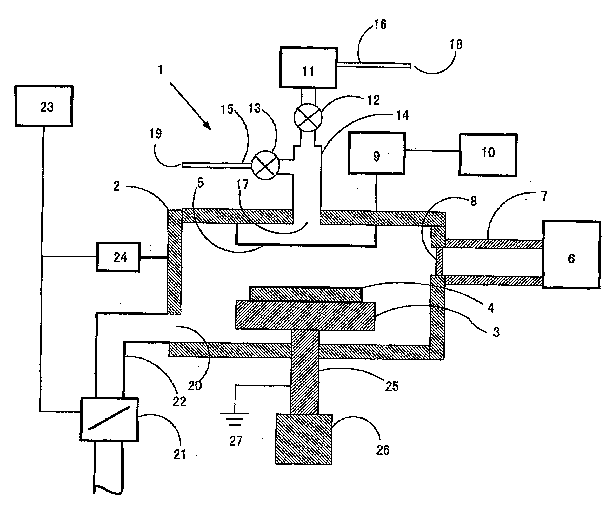
[0045]FIG. 1 indicates an embodiment of a thin-film deposition apparatus according to the present invention. A semiconductor substrate 4, onto which a carbon-containing silicon oxide film or a silicon carbide film is deposited, is placed on a susceptor heater 3 set up inside a reactor 2. Inside the reactor 2, a showerhead 5 used for feeding a reaction gas into a reactor 5 is set up in a position opposing to the susceptor heater 3. The susceptor heater 3, in which a resistance-heating-type sheath heater (not shown) and a temperature sensor (not shown) are embedded, is kept at constant high temperature by an external temperature controller (not shown). The heated susceptor heater 3 heats the semiconductor substrate 4 to a given appropriate temperature appropriate for film deposition. In the reactor 2, an exhaust port 20 for evacuating the interior of the reactor is provided and is connected to a vacuum pump (not shown) t...


PUM

PropertyMeasurementUnit
Poweraaaaaaaaaa

Abstract

A thin-film deposition system includes a plasma CVD reactor; a remote plasma chamber; and an electromagnetic wave generator for emitting electromagnetic waves to an interior of the reactor. Unwanted reaction products adhering to an inner surface of the reactor absorb electromagnetic waves are effectively removed.

Description

BACKGROUND OF THE INVENTION [0001] 1. Field of the Invention [0002] This invention relates generally to a method for cleaning a plasma CVD (chemical vapor deposition) reactor and a plasma CVD apparatus provided with a cleaning device. [0003] 2. Description of the Related Art [0004] In a single-substrate- or small-batch substrate-processing system, during CVD processing, a film is formed not only on a substrate but also on inner walls or other inner parts of a CVD chamber. An unwanted film formed on the inner parts of the chamber produces particles which fall on a substrate during CVD processing and degrade the quality of a film on the substrate. Thus, the CVD chamber is cleaned periodically by using an in-situ cleaning process to remove unwanted adhesive products from an inner surface of the CVD chamber. [0005] In conventional LSI (large scale integration) devices such as CPU, memory, and system LSI, an insulator formed between metal lines is typically silicon dioxide (SiH4-based Si...

Claims


Application Information

Patent Timeline
IPC IPC(8): B05D3/14C23C16/00C23C16/44C23C16/32C23C16/40H01L21/205
CPCC23C16/325C23C16/4405C23C16/401
Inventor LOKE, CHOU SAN NELSONKAGAMI, KENICHISATOH, KIYOSHI
Owner ASM JAPAN
Why Eureka
Try Eureka