Monolithic integration and enhanced light extraction in gallium nitride-based light-emitting devices

Inactive Publication Date: 2005-08-18
KOPIN CORPORATION
View PDF99 Cites 36 Cited by
  • Summary
  • Abstract
  • Description
  • Claims
  • Application Information

AI Technical Summary

Benefits of technology

[0016] With the integrated light-emitting devices of the invention, multiple p-n diodes, either all light-emitting diodes or light-emitting diode(s) in combination with ESD protection didoe(s), are monolithically integrated on a single insulating substrate. The present invention, thus, provides much simpler and more reliable solution than the use of multiple discrete p-n diodes connected by wire-bonding or bump-bonding. Also, the present invention is advantageous over the conventional integration of discrete p-n diodes by wire-bonding or bump-bonding, because multiple p-n diodes are integrated monolithically before packaging, reducing the total number of terminals connected in the package.
[0017] In addition, by beveling at least one sidewall of light-emitting device, enhanced light extraction can be achieved. In particular, the integrated device of one embodiment of the invention, where multipl

Problems solved by technology

However, as GaN-based light-emitting devices become utilized in diverse applications, it becomes challenging for a traditional single p-n diode structure to meet the requirements of these diverse applications.
Typically, in the light-emitting devices, ESD is caused by the imbalance of electrical charges at interfaces between the light-emitting devices and other external environments.
This ESD can cause a catastrophic device failure by an electrical overstress, causing a larger amount of current to flow through the device than it can tolerate.
Using two discrete components to provide ESD protection, however, req

Method used


Image

  • Monolithic integration and enhanced light extraction in gallium nitride-based light-emitting devices
  • Monolithic integration and enhanced light extraction in gallium nitride-based light-emitting devices
  • Monolithic integration and enhanced light extraction in gallium nitride-based light-emitting devices

Examples


example 1

Deposition of GaN-Based Semiconductor Layers on a Sapphire Substrate

[0069] Semiconductor layers were grown in a c-sapphire substrate by low-pressure MOCVD. The first deposited layer was a 20 nm-thick GaN nucleation layer, which was followed by a 4 μm-thick, silicon-doped (doping concentration of about 1019 cm−3) n-type GaN layer. The next layers were multiple quantum well active layers made of InxGa1-xN / GaN (017 cm−3, as determined by the Hall measurement. After the MOCVD growth of the epitaxial layers, the device fabrication was carried out using conventional semiconductor processing techniques commonly used in industry.

example 2

Device Fabrication: Monolithic Integration For ESD Protection

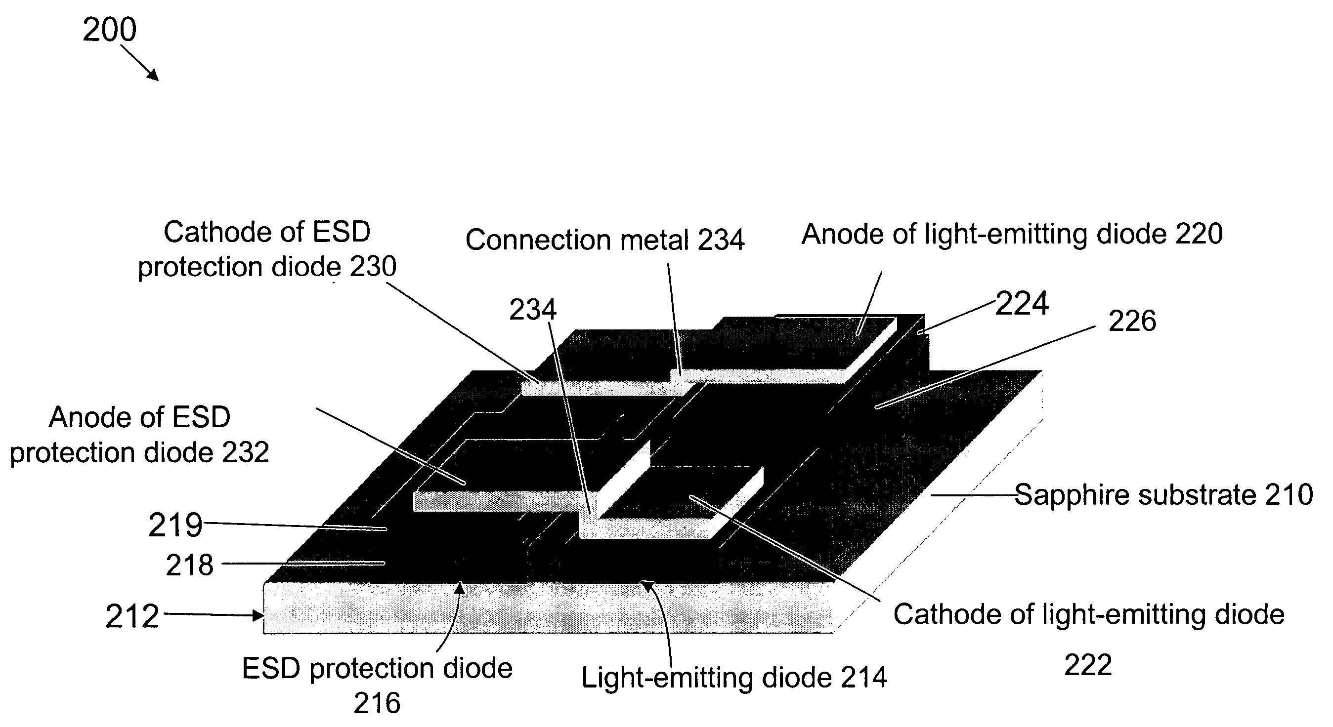
[0070] Using the semiconductor layers grown as described in Example 1, an integrated light-emitting device that includes a light-emitting diode and an ESD protection diode was monolithically fabricated. The integrated light-emitting device was fabricated following the schematic of the integration shown FIG. 4. The definition of two junction areas and the subsequent device isolation were achieved by ICP etching processes. Transparent contact layers based either on nickel-oxide (see U.S. Pat. No. 6,734,091) or on indium-oxide (see Attorney Docket Number 0717.2048-000) were deposited on top of the p-n junction areas to enhance the current spreading throughout the p-type GaN layers. In order not to short the diodes an insulating layer of silicon dioxide was deposited by plasma enhanced chemical vapor deposition (PECVD) on the whole surface. Openings were made in silicon dioxide layer by a chemical wet etching only in the area...

example 3

Device Fabrication: Monolithic Integration For ESD Protection with a Relatively Small-Sized ESD-Protection Diode

[0073]FIG. 5 shows another example of the monolithic integration of a light-emitting diode and an ESD protection diode. The ESD protection diode in this example was made much smaller than that of Example 2 in order to minimize the increase in the operating voltage and the decrease in the light output. The fabrication process was the same as those of Example 2. The finished device size was 300×300 μm 2. During the test of the ESD tolerance in HBM, 100% of the devices with two diodes that were tested showed endurance against HBM up to 1000V. Hundred samples were tested for each device, i.e., the integrated device of the invention and control device. This result confirms an improvement in the ESD endurance as a result of the monolithic integration with a much smaller size protection diode. Due to the small size of the protection diode, the forward operating voltage and the l...


PUM


Abstract

An integrated light-emitting device includes multiple p-n diodes integrated monolithically on an insulating substrate. The p-n diodes are of monolithic semiconductor materials over the single substrate. The p-n diodes can be all light-emitting diodes or a combination of light-emitting and ESD-protection diodes. The p-n diodes may have at least one beveled sidewall to enhance light extraction out of the light-emitting diodes. A method for producing such integrated light-emitting device and a method for producing such p-n diode that includes at least one beveled sidewall are also disclosed.

Description

RELATED APPLICATIONS [0001] This application claims the benefit of U.S. Provisional Application No. 60 / 544,577, filed on Feb. 13, 2004. This application also claims the benefit of U.S. Provisional Application Nos. 60 / 553,718 and 60 / 553,717, both of which were filed on Mar. 15, 2004. The entire teachings of the above applications are incorporated herein by reference.BACKGROUND OF THE INVENTION [0002] In general, gallium nitride (GaN)-based light emitting devices are based on a p-n diode structure including n-type and p-type GaN-based semiconductor layers stacked on top of a substrate through a process of epitaxial or domain epitaxial growth. A GaN-based light-emitting device with a traditional single p-n diode structure has been widely utilized as an efficient light source for realizing such colors as blue, green, and white. However, as GaN-based light-emitting devices become utilized in diverse applications, it becomes challenging for a traditional single p-n diode structure to meet...

Claims


Application Information

Patent Timeline
IPC IPC(8): H01L27/15H01L33/20
CPCH01L33/20H01L27/153
Inventor YANG, BOOH, TCHANG-HUNDINGLE, BRENDAROBERTS, WILLIAM T.LIBENZON, ILYACHOI, HONG K.FAN, JOHN C. C.
Owner KOPIN CORPORATION
Why Eureka
Try Eureka