Solid state imaging device and method of fabricating the same

Inactive Publication Date: 2005-08-18
FUJIFILM CORP
View PDF2 Cites 1 Cited by
  • Summary
  • Abstract
  • Description
  • Claims
  • Application Information

AI Technical Summary

Benefits of technology

[0036] After the silicidation, the non-silicidated metal film is removed by etching. In this embodiment, the photolithographic step or the etching step necessary to form a low resistance layer, such as a metal layer, is not needed. Thus, the number of steps involved is reduced, and the yield is improved thereby.
[0037] The step of forming a silicon-based conductive film preferably comprises the substeps of forming a polycrystalline silicon film a

Problems solved by technology

A silicon oxide film formed by thermal oxidation of polycrystalline silicon is poor in film quality compared with that formed by chemical vapor deposition (CVD).
A solid state imaging device having such a thermally oxidized insulating film between the electrodes is more liable to suffer from a short circuit as the electrode pattern becomes finer.
When the interelectrode insulating film i

Method used


Image

  • Solid state imaging device and method of fabricating the same
  • Solid state imaging device and method of fabricating the same
  • Solid state imaging device and method of fabricating the same

Examples


Embodiment Construction

[0054] The preferred embodiments of the present invention will be described with reference to the accompanying drawings.

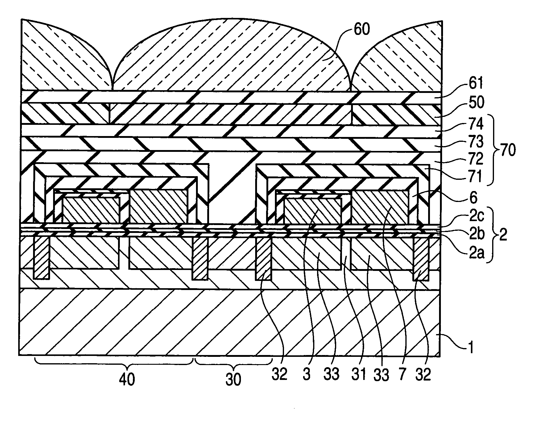
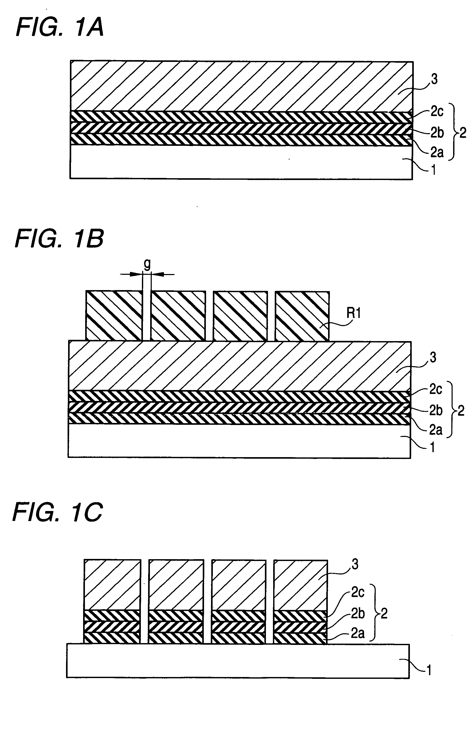
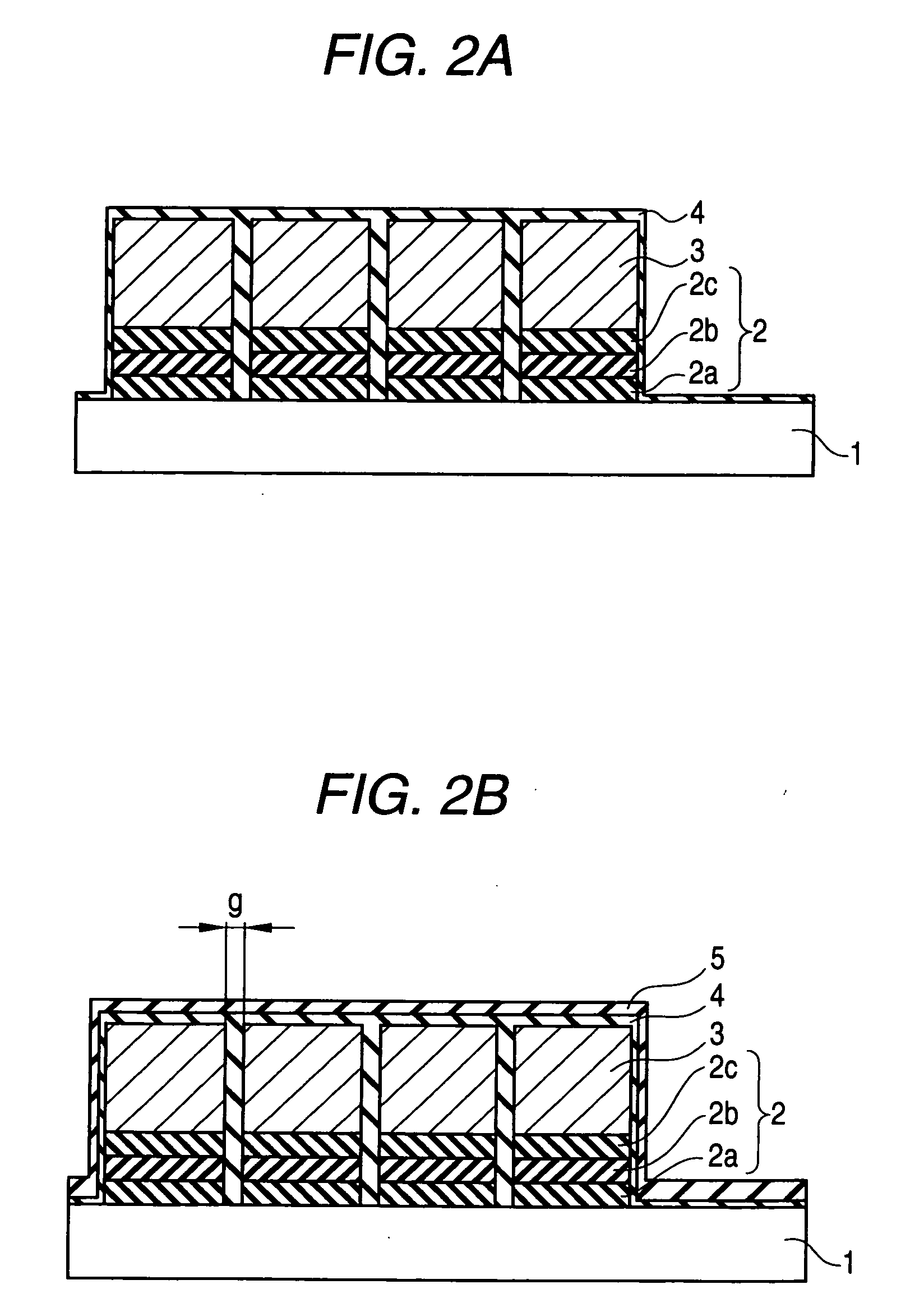
[0055]FIGS. 1 through 3 represent a method of fabricating a solid state imaging device according to a first embodiment of the invention.

[0056] The method is characterized by the process of forming the electrodes separated with a small interelectrode spacing and filling the interelectrode spacings with an interelectrode insulating film of silicon oxide by vacuum CVD as shown in FIGS. 1 and 2. FIGS. 3 and 4 show a schematic plan view and a schematic cross-sectional view, respectively, of the solid state imaging device produced by the method.

[0057] In the first embodiment, the gap g, the interelectrode distance, is set at 0.2 μm. In such narrow interelectrode gaps is formed an interelectrode insulating film 4 of silicon oxide by vacuum CVD. The silicon oxide insulating film 4 formed by vacuum CVD exhibits satisfactory film qualities.

[0058] The openings with such a...


PUM


Abstract

A method for fabricating a solid state imaging device comprising photoelectric conversion sections and charge transfer sections having single-layered charge transfer electrodes for transferring charges generated in the photoelectric conversion sections, the method including formation of the charge transfer electrodes, wherein the formation of the charge transfer electrodes comprises the steps of: forming a conductive film on a surface of a semiconductor substrate having formed thereon a gate oxide film; forming a mask pattern on the conductive film; forming interelectrode spacings in the conductive film using the mask pattern as a mask to make a patterned conductive film; and forming an insulating film to fill in the interelectrode spacings by vacuum chemical vapor deposition.

Description

FIELD OF THE INVENTION [0001] This invention relates to a solid state imaging device and a method of fabricating the same. In particularly, it relates to an interelectrode insulating film of a solid state imaging device featuring a CCD (charge coupled device) structure having single-layered electrodes. BACKGROUND OF THE INVENTION [0002] A CCD solid state imaging device useful as an area sensor, etc. has photoelectric conversion sections, such as photodiodes, and charge transfer sections having charge transfer electrodes for transferring signal charges from the photoelectric conversion sections. The charge transfer electrodes are arranged on charge transfer paths formed in a semiconductor substrate and driven by successive voltage application. [0003] In recent years, the pixel count of solid state imaging devices has been increasing to giga pixels or even greater. With an increase of pixels, it is required to transfer signal charges at a higher speed, i.e., to drive charge transfer e...

Claims


Application Information

Patent Timeline
IPC IPC(8): H01L21/00H01L29/762H01L21/339H01L27/146H01L27/148H01L31/062H04N5/335H04N5/369H04N5/372H04N5/374
CPCH01L27/14687H01L29/66954H01L27/14806
Inventor TAKAO, HIROAKI
Owner FUJIFILM CORP
Why Eureka
Try Eureka