Liquid crystal display device

a liquid crystal display and active matrix technology, applied in static indicating devices, fire alarms, instruments, etc., can solve the problems of the difficulty in connecting the liquid crystal display section with the liquid crystal drive circuit, etc., to reduce the load of the signal source, increase the operating speed of the drive circuit, and low power consumption

Inactive Publication Date: 2005-08-25
SHARP KK
View PDF31 Cites 29 Cited by
  • Summary
  • Abstract
  • Description
  • Claims
  • Application Information

AI Technical Summary

Benefits of technology

[0035] The present invention was made to solve the above problems, and an object of the present invention is to provide a liquid crystal display device that achieves increase in operating speed of a drive circuit, reduction in load of signal source, low power consumption, and improvement in reliability of electric conduction between a liquid crystal display section and a liquid crystal driver.

Problems solved by technology

This causes a difficulty in connecting the liquid crystal display section with the liquid crystal drive circuit.
However, in the drive methods disclosed in Document 1 and Document 2, if the number of pixels is increased to a further greater value, as well as the number of source signal lines and the number of gate signal lines, there again occurs the problem of difficulty in connecting the liquid crystal display section with the liquid crystal driver.
Meanwhile, when all the drive circuits are formed on the glass substrate as disclosed in Document 3, the following problem occurs.
On this account, the liquid crystal drive circuit formed on the glass substrate is slower in operating speed, and therefore, lower in driving ability than the liquid crystal drive circuit (LSI) formed on the silicon substrate.
Such decrease in operating speed of the liquid crystal drive circuit results in incapability of processing of data signals at a predetermined sampling speed.
Therefore, the load of the signal source increases.
Therefore, electric power consumption is increased (see Non-patent Document 2).
In the structure disclosed in Document 3, these problems are ineludible in forming all the drive circuits on the glass substrate.

Method used


Image

  • Liquid crystal display device
  • Liquid crystal display device
  • Liquid crystal display device

Examples


embodiment 1

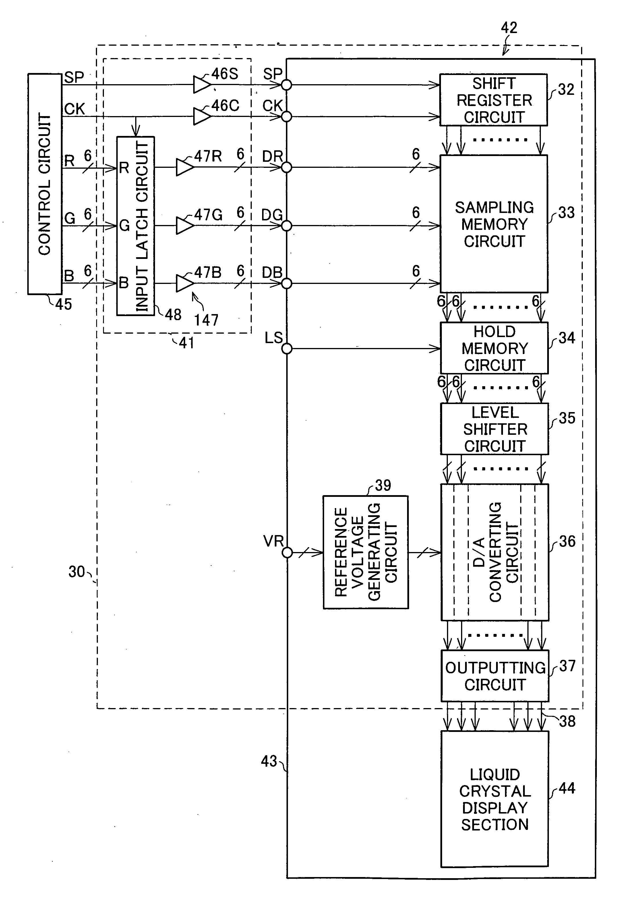
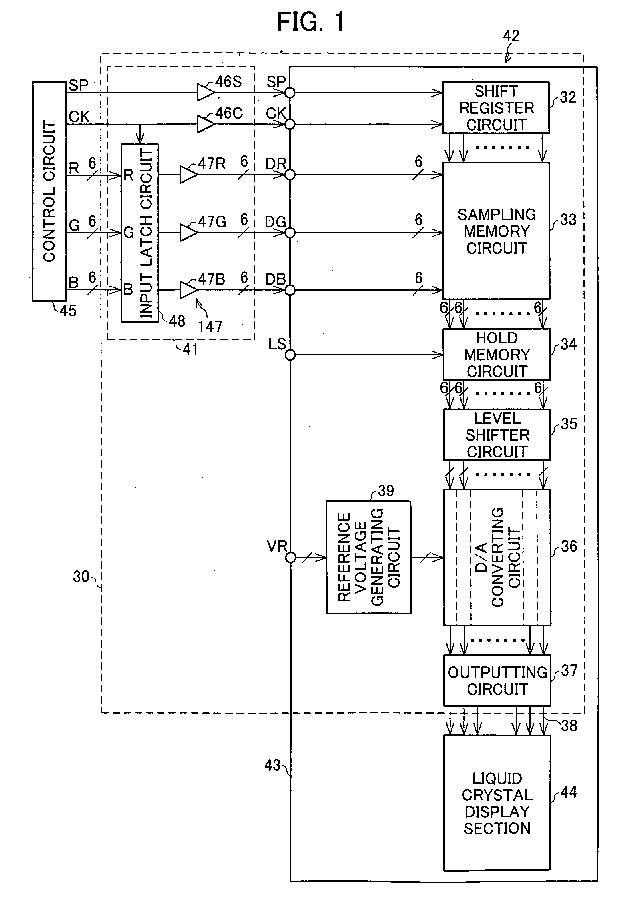
[0050] The following description explains one embodiment of the present invention in reference to the figures. FIG. 1 is a block diagram illustrating an arrangement of a TFT type liquid crystal display device as the liquid crystal display device in accordance with one embodiment of the present invention, which carries out display by driving display data by an LSI.

[0051] As described above, when all circuits for performing the functions of respective blocks of FIG. 8 are formed on a glass substrate, various problems occur. That is, because the input capacity of input buffer of each of the circuits on the glass substrate is large, and display data D is inputted in parallel to n source drivers as illustrated in FIG. 4, a high driving ability is required for the output section of a controller 5 outputting the display data D. Moreover, because a transfer rate from the controller 5 to the circuits on the glass substrate is high, when a data signal from the controller 5 is transferred dir...

embodiment 2

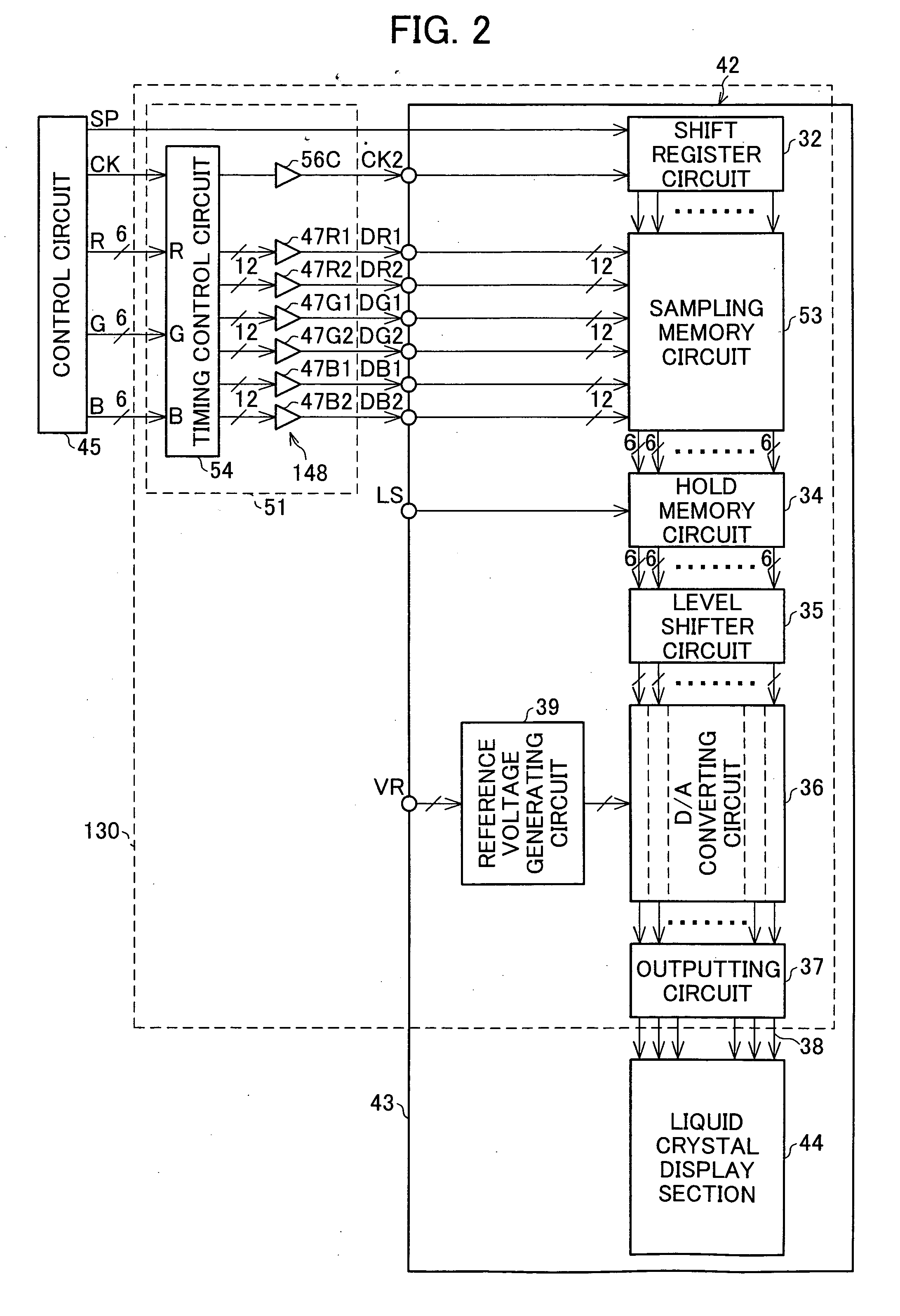
[0073] The following description explains another embodiment of the present invention in reference to the figures. Note that, for ease of explanation, the same reference numerals are used for the members having the same functions as the members used in Embodiment 1, and further explanations thereof are omitted.

[0074] As described above, operations of the circuits formed on a glass substrate (circuits contained in the liquid crystal display panel) are slower than operations of the circuits formed on a monocrystal silicon substrate. Therefore, the circuits contained in the liquid crystal panel may fail to cope with the speed of the clock signal CK used for sampling the display data. This may result in failure of proper sampling.

[0075] In order to solve such a problem, in the liquid crystal display device in accordance with the present embodiment, a data sampling speed of the circuits contained in the liquid crystal panel is adjusted to be one half of a data sampling speed according ...


PUM

PropertyMeasurementUnit
electron mobilityaaaaaaaaaa
driving voltageaaaaaaaaaa

Abstract

The present invention provides a liquid crystal display device that achieves increase in operating speed of a drive circuit, reduction in load of signal source, low power consumption, and improvement in reliability of electric conduction between a liquid crystal display section and a liquid crystal driver. The liquid crystal display device includes a liquid crystal display section 44, a source driver 30 having an input latch circuit 48 and circuits 33 to 37, and 39 each of which samples gradation displaying data signal R,G, or B outputted from a control circuit 45 and holds the signal in output terminals thereof for a predetermined period. The circuits 33 to 37, and 39 are each formed of a p-Si thin film on a glass substrate 43 on which the liquid crystal display section 44 is provided. Moreover, the input latch circuit 48 is formed inside a logic circuit 41 formed on a monocrystal silicon substrate.

Description

[0001] This Nonprovisional application claims priority under 35 U.S.C. § 119(a) on Patent Application No. 2004 / 43570 filed in Japan on Feb. 19, 2004, the entire contents of which are hereby incorporated by reference. FIELD OF THE INVENTION [0002] The present invention relates to an active matrix liquid crystal display device such as a TFT (Thin Film Transistor) liquid crystal display device, and particularly relates to an active matrix liquid crystal display device in which at least a part of a liquid crystal drive circuit, which applies a gradation displaying analog voltage to a liquid crystal pixel, is formed on a substrate such as a glass substrate on which switching sections such as TFTs and liquid crystal are formed. BACKGROUND OF THE INVENTION [0003] Conventionally, an active matrix type liquid crystal display device is generally arranged such that a liquid crystal display section including liquid crystal, switching sections, and the like is formed on a glass substrate, and a ...

Claims


Application Information

Patent Timeline
Patent Type & Authority Applications(United States)
IPC IPC(8): G02F1/133G02F1/136G09G3/20G09G3/36G09G5/00
CPCG09G5/006G09G3/3688G09G2310/027G08B17/06G08B17/117G08B21/16H04B1/40
Inventor SAKAGUCHI, NOBUHISA
Owner SHARP KK
Why Eureka
Try Eureka