SONOS embedded memory with CVD dielectric

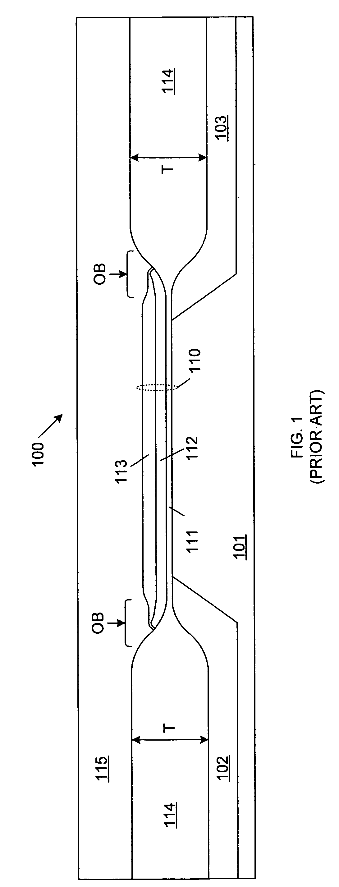
a dielectric and embedded memory technology, applied in the field of semiconductor device fabrication, can solve the problems of poor dielectric performance in the oxybeak region, the process steps required to fabricate high, medium and low voltage cmos logic transistors are not fully compatible with the process steps required to fabricate fieldless array transistors, and the leakage current of transistors and diodes is typically increased, so as to achieve the effect of fast ra

Inactive Publication Date: 2005-08-25
PS4 LUXCO SARL
View PDF9 Cites 74 Cited by
  • Summary
  • Abstract
  • Description
  • Claims
  • Application Information

AI Technical Summary

Benefits of technology

[0015] The embedded semiconductor-memory device is fabricated in the following manner. Shallow trench isolation regions are typically fabricated in the CMOS region of the device. Diffusion bit line regions are then formed in the fieldless array region of the semiconductor substrate. The upper surface of the substrate is then thermally oxidized, thereby forming the bottom oxide layer over the substrate and simultaneously forming bit line oxide regions over each of the diffusion bit line regions. The bit line oxide regions, which are more heavily doped than the other regions of the substrate, enable the bit line oxide regions to grow at a faster rate than the bottom oxide layer. For example, the bit line oxide regions may grow 2 to 3 times faster than the bottom oxide layer. In one embodiment, the bottom oxide layer has a thickness of about 50 Angstroms, and the bit line oxide regions have a thickness of about 100 to 150 Angstroms. This is significantly thinner than conventional bit line oxide regions.

Problems solved by technology

The process steps required to fabricate high, medium and low voltage CMOS logic transistors are not fully compatible with the process steps required to fabricate fieldless array transistors.
As a result, transistor and diode leakage currents will typically increase.
This results in poor dielectric performance in the oxybeak region and directly influences the reliability of the resulting memory device.
This consumption of the bit line oxide can result in a stressed oxybeak region.
As a result, the charge-to-breakdown (Qbd) values of the fieldless array transistors are low even with the high temperature top oxide layer.

Method used


Image

  • SONOS embedded memory with CVD dielectric
  • SONOS embedded memory with CVD dielectric
  • SONOS embedded memory with CVD dielectric

Examples


Embodiment Construction

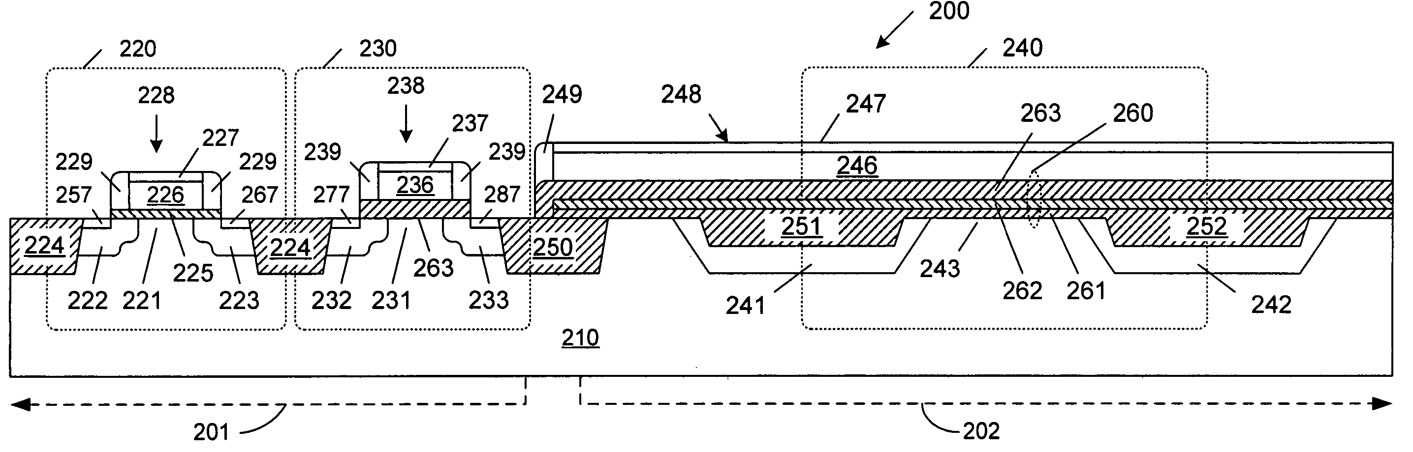
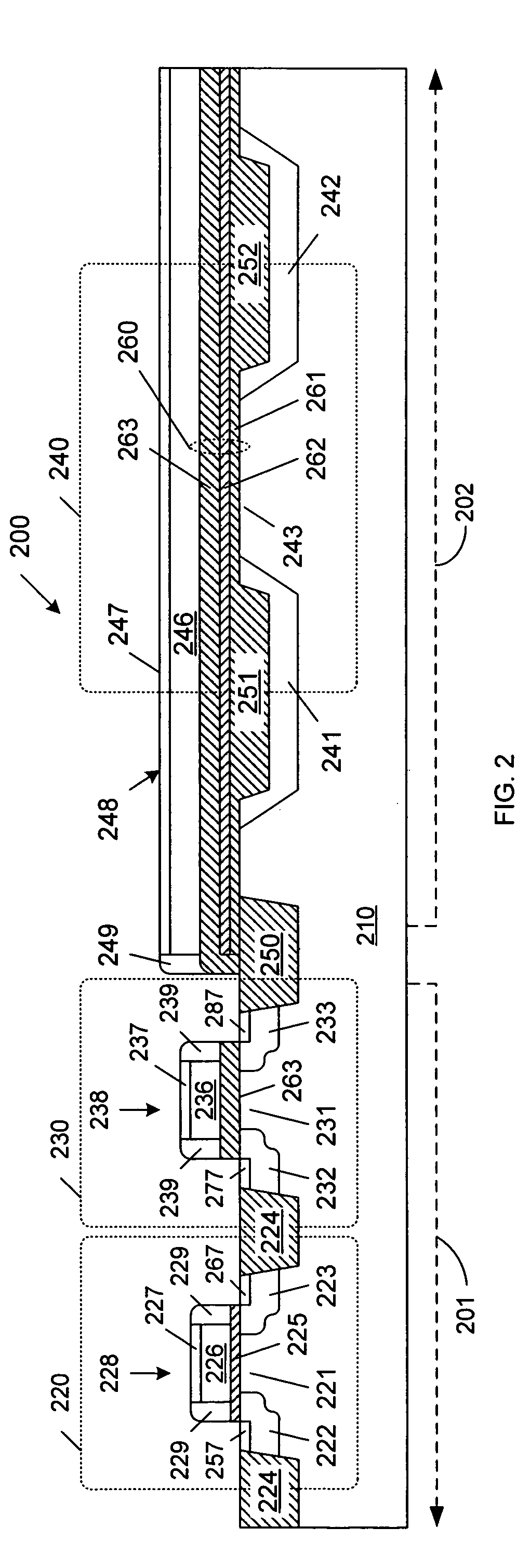
[0022] In accordance with the present invention, the top oxide layer of an ONO memory stack and the gate oxide of a high voltage logic transistor are formed by depositing a high temperature CVD oxide. The high temperature CVD oxide eliminates the requirement of thermally growing high-voltage gate oxide for the high voltage logic transistors. Because the high-voltage gate oxide is not thermally grown, the critical influence of a high-temperature thermal oxidation on shallow trench isolation regions of the device is eliminated. Eliminating the thermal growth of the high voltage gate oxide also decreases the number of operations and masks in the process flow, because there is no need for additional masking of the bit line oxide during the CMOS oxide fabrication. In addition, the silicon nitride layer of the ONO stack serves as protection against bit line oxide loss during the CMOS part processing.

[0023] The present invention provides a reliable oxybeak region in a process that uses hi...


PUM


Abstract

An embedded semiconductor memory is fabricated by: forming diffusion bit line regions in a semiconductor substrate; then thermally oxidizing the upper surface of the substrate, thereby forming a bottom oxide layer over the substrate and simultaneously forming bit line oxide regions over each of the diffusion bit line regions; and then forming an intermediate dielectric layer (e.g., silicon nitride), over the bottom oxide layer and the bit line oxide regions. CMOS well implants are then performed in a CMOS section of the device through the silicon nitride layer and bottom oxide layer. The silicon nitride layer and bottom oxide layer are then removed in the CMOS section, and a top dielectric layer, such as a high-temperature oxide or a high-k dielectric, is deposited. The top dielectric layer completes a memory stack of the memory device, and forms a gate dielectric layer of a high voltage transistor in the CMOS section.

Description

FIELD OF THE INVENTION [0001] The present invention relates to the fabrication of a semiconductor device. More specifically, the present invention relates to a method of fabricating a semiconductor device that includes a first region containing CMOS logic devices and a second region containing a fieldless array of memory transistors having a silicon-oxide-nitride-oxide-silicon (SONOS) structure. BACKGROUND OF THE INVENTION [0002] In many memory applications, SONOS memory transistors and conventional CMOS devices are fabricated on a single semiconductor wafer. Typically, the CMOS devices are fabricated in a first region of the wafer, while the SONOS memory transistors are fabricated in a second region of the wafer. On some wafers, the SONOS memory transistors are fabricated as part of a fieldless array. A fieldless array is defined as an array that does not use field oxide or shallow trench isolation (STI) to isolate the various elements of the array. Because field oxide and / or STI i...

Claims


Application Information

Patent Timeline
Patent Type & Authority Applications(United States)
IPC IPC(8): H01L21/8234H01L21/8238H01L21/8239H01L21/8246H01L21/8247H01L27/105
CPCH01L27/105H01L27/11521H01L27/1052H01L27/11573H01L27/11568H10B99/00H10B41/30H10B43/30H10B43/40
Inventor ROIZIN, YAKOVSHTERENFELD-LAVIE, ZMIRAEDREI, ITZHAK
Owner PS4 LUXCO SARL
Why Eureka
Try Eureka