Controlled cleaving process

Inactive Publication Date: 2005-08-25
SILICON GENERAL CORPORATION
View PDF99 Cites 11 Cited by
  • Summary
  • Abstract
  • Description
  • Claims
  • Application Information

AI Technical Summary

Benefits of technology

[0009] According to the present invention, an improved technique for removing a thin film of material from a substrate using a controlled cleaving action is provided. This technique allows an initiation of a cleaving process on a substrate using a single or mul

Problems solved by technology

This technique, however, is often extremely “rough” and cannot generally be used for providing precision separations in the substrate for the manufacture of fine tools and assemblies.
Additionally, the saw operation often has difficulty separating or cutting extremely hard and/or brittle materials, such as diamond or glass.
Although the techniques described above are satisfactory, for the most part, as applied to cutting diamonds or household glass, they have severe limitations in the fabrication of small complex structures or precision workpieces.
For instance,

Method used


Image

  • Controlled cleaving process
  • Controlled cleaving process
  • Controlled cleaving process

Examples


Example

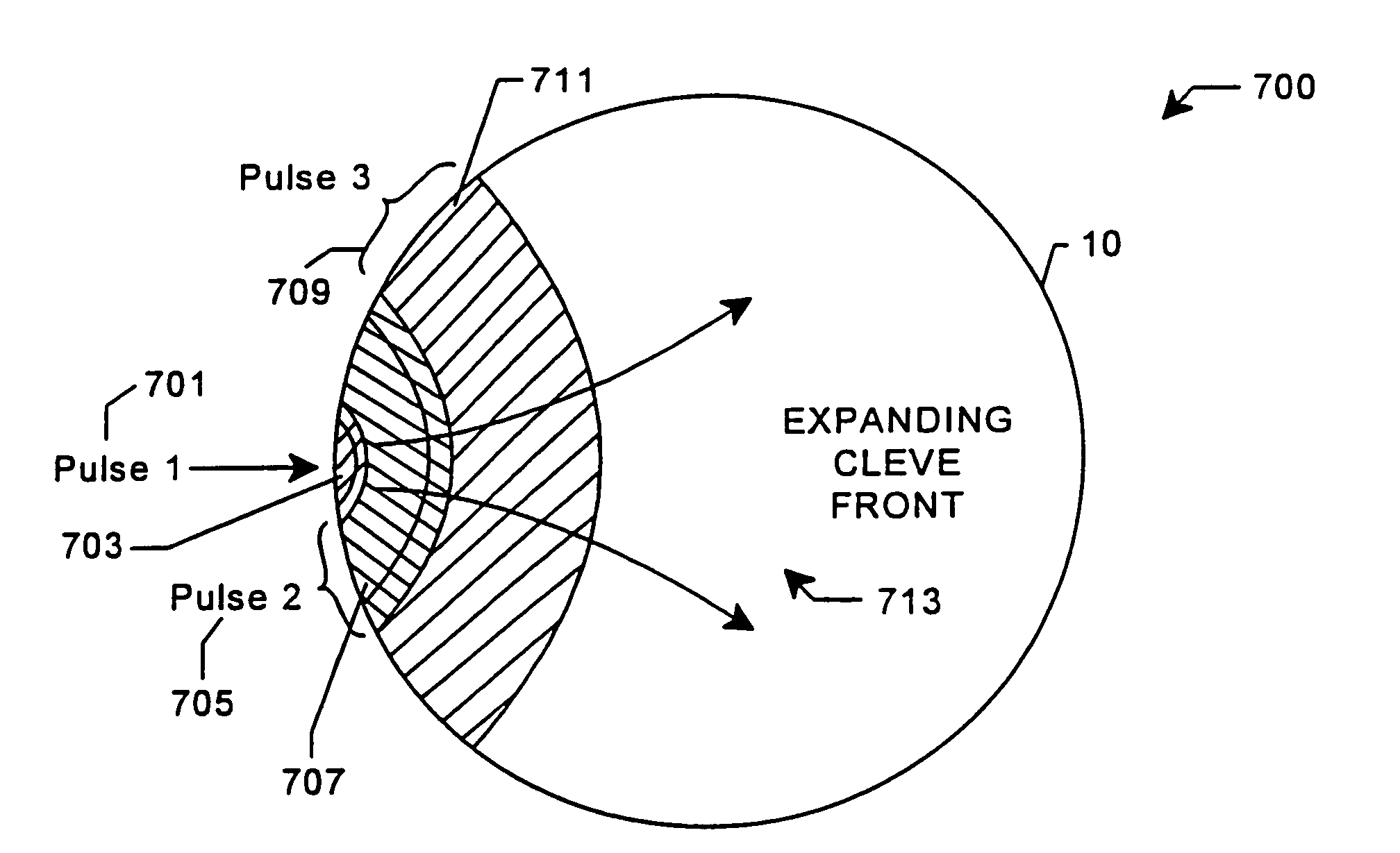
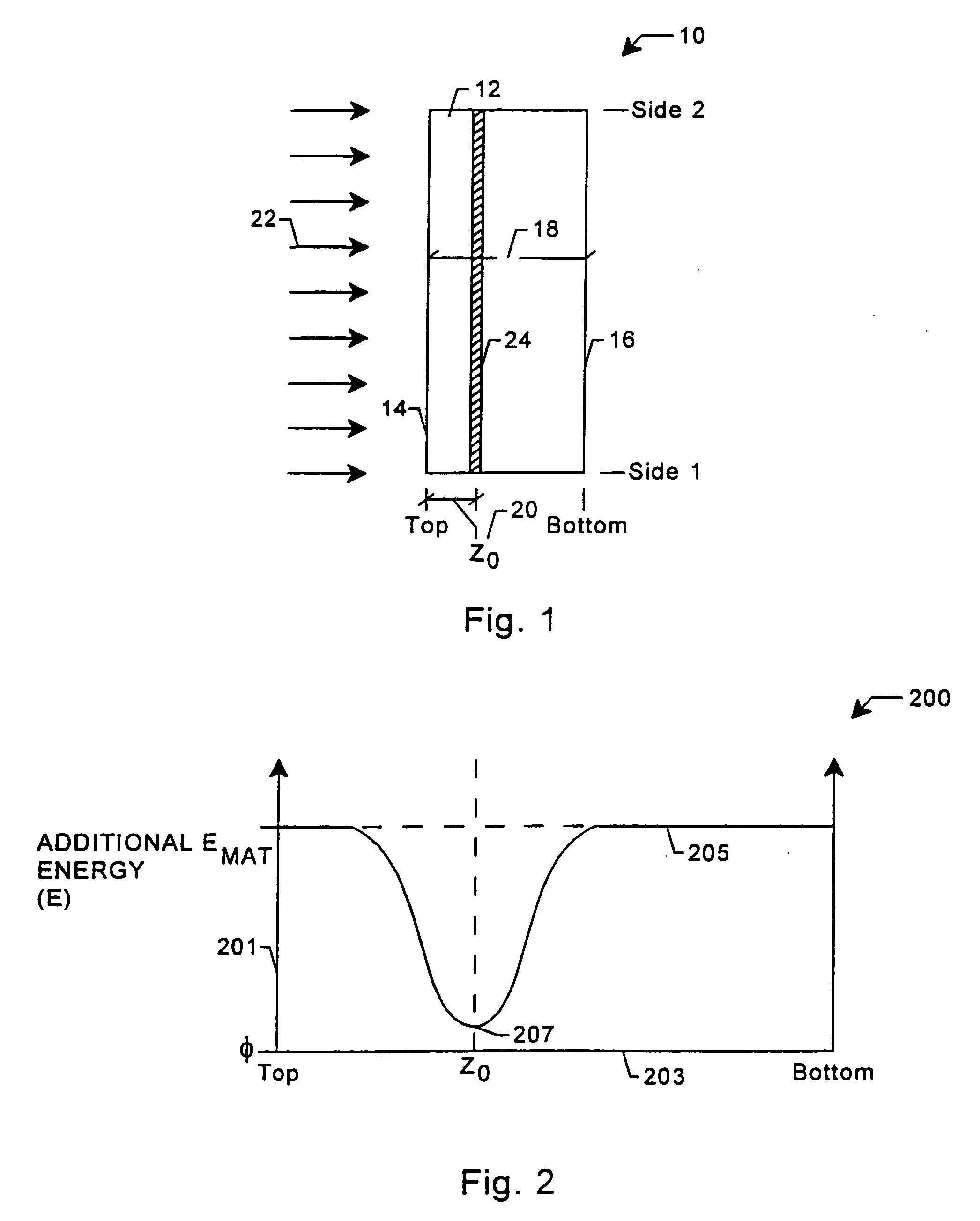
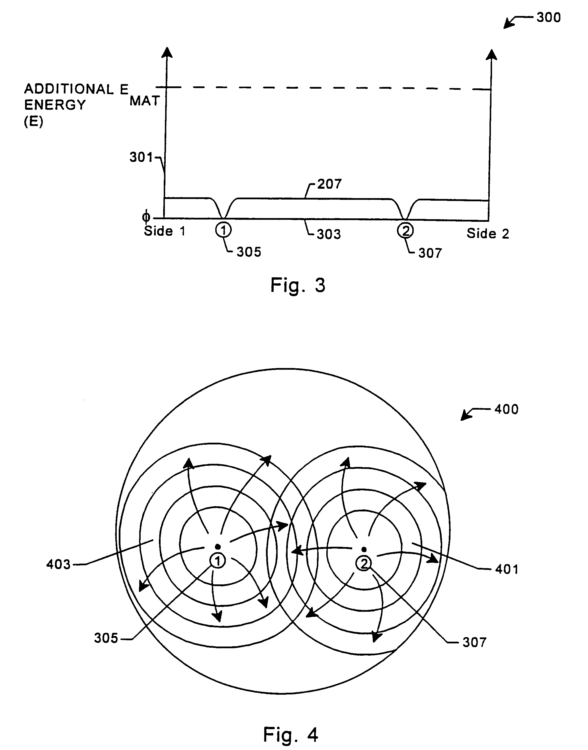
[0021] The present invention provides a technique for removing a thin film of material from a substrate while preventing a possibility of damage to the thin material film and / or a remaining portion of the substrate. The thin film of material is attached to or can be attached to a target substrate to form, for example, a silicon-on-insulator wafer. The thin film of material can also be used for a variety of other applications. The invention will be better understood by reference to the Figs. and the descriptions below.

[0022] 1. Controlled Cleaving Techniques

[0023]FIG. 1 is a simplified cross-sectional view diagram of a substrate 10 according to the present invention. The diagram is merely an illustration and should not limit the scope of the claims herein. As merely an example, substrate 10 is a silicon wafer which includes a material region 12 to be removed, which is a thin relatively uniform film derived from the substrate material. The silicon wafer 10 includes a top surface 14,...


PUM

PropertyMeasurementUnit
Dielectric polarization enthalpyaaaaaaaaaa
Electrical conductoraaaaaaaaaa
Plasticityaaaaaaaaaa

Abstract

A technique for forming a film of material (12) from a donor substrate (10). The technique has a step of introducing energetic particles (22) through a surface of a donor substrate (10) to a selected depth (20) underneath the surface, where the particles have a relatively high concentration to define a donor substrate material (12) above the selected depth. An energy source is directed to a selected region of the donor substrate to initiate a controlled cleaving action of the substrate (10) at the selected depth (20), whereupon the cleaving action provides an expanding cleave front to free the donor material from a remaining portion of the donor substrate.

Description

CROSS REFERENCE TO RELATED APPLICATIONS [0001] This application claims priority from the provisional patent application entitled A CONTROLLED CLEAVAGE PROCESS AND RESULTING DEVICE, filed May 12, 1997 and assigned Application No. 60 / 046,276, the disclosure of which is hereby incorporated in its entirety for all purposes.BACKGROUND OF THE INVENTION [0002] The present invention relates to the manufacture of substrates. More particularly, the invention provides a technique including a method and device for cleaving a substrate in the fabrication of a silicon-on-insulator substrate for semiconductor integrated circuits, for example. But it will be recognized that the invention has a wider range of applicability; it can also be applied to other substrates for multi-layered integrated circuit devices, three-dimensional packaging of integrated semiconductor devices, photonic devices, piezoelectronic devices, microelectromechanical systems (“MEMS”), sensors, actuators, solar cells, flat pane...

Claims


Application Information

Patent Timeline
IPC IPC(8): B24C1/00B26F3/00B26F3/02B32B5/16B81C1/00H01L21/00H01L21/18H01L21/20H01L21/22H01L21/223H01L21/265H01L21/30H01L21/301H01L21/302H01L21/304H01L21/36H01L21/38H01L21/425H01L21/44H01L21/46H01L21/461H01L21/48H01L21/50H01L21/762H01L21/78H01L21/8238
CPCB81C1/0038Y10T428/21B81C2201/0192H01L21/187H01L21/2007H01L21/2236H01L21/26506H01L21/304H01L21/7624H01L21/76254H01L21/7813Y10S156/93Y10S117/915Y10S438/977Y10S438/974Y10T156/1158Y10T156/19Y10T156/11Y10T428/24893B81C2201/0191Y10T428/249956H01L21/2658H01L21/02376H01L21/02381H01L21/02387H01L21/265
Inventor HENLEY, FRANCOIS J.CHEUNG, NATHAN W.
Owner SILICON GENERAL CORPORATION
Why Eureka
Try Eureka