Method for analyzing and validating clock integration properties in circuit systems

a technology of clock integration and circuit system, applied in the direction of cad circuit design, program control, instruments, etc., can solve the problems of increasing the number of distinct clock domains, increasing the complexity of the number of clock domains, and presenting many challenges to the development team of soc designs, so as to improve capacity and consume less memory and runtime

Inactive Publication Date: 2005-09-08
PICOCRAFT DESIGN SYST
View PDF5 Cites 82 Cited by
  • Summary
  • Abstract
  • Description
  • Claims
  • Application Information

AI Technical Summary

Benefits of technology

[0019] The present invention provides a number of key advantages over current functional and static timing analysis tools by having improved capacity. Specifically, the present invention consumes less memory and runtime than current methods for the same design. Both the timing point frame and the clock analysis view are condensed representations as compared to a full gate level netlist specification. Accordingly, for a computer's given processing speed and memory capacity, larger designs can be analyzed on the same schedule as the current timing analysis tools. As such, the present invention can be used to analyze an entire chip at once, as opposed to partial designs.
[0020] The present invention also provides thorough analysis with little user guidance thereby significantly reducing the risk that an error in the timing and clocking specification of the design will escape the designer's notice. The present invention does not require the designer to specify input stimulus as is required for a functional simulation. The static nature of path traversal used in collapsing non-clocked cells during the construction of the timing point frame in the present invention ensures path completeness and is further abstracted into the clock analysis view.

Problems solved by technology

But the highly integrated nature of SOC designs present many challenges to development teams.
These changes, although they should leave the circuit functionally equivalent to its logical design phase specification, may re-arrange or even disperse clock domains that were once local thereby resulting in additional delays that can directly impact both effective clock operating frequencies and clock domain interactions.
Analyzing the impact of these physical design phase specification refinements and validating that the chip will still meet performance objectives is greatly complicated in both VLSI and SOC chips due to their typically high clock counts.
It's not enough to simply validate each clock, a problem that scales linearly with the clock count, but the designer must also validate clock domain interactions across all of the distinct operating conditions and test modes of the chip.
This is a challenge that has exponentially increasing complexity with the number of distinct clock domains increasing.
If functional simulation is the only method employed to analyze clock interactions, it is possible that all required checks for all relevant scenarios may not be performed.
In addition, selecting all of the appropriate probe points to correctly observe the interaction between clock domains in the functional simulation is extremely challenging.
An error may be missed even if a complete set of stimulus vectors are offered.
There are key limiting factors to the usefulness of static timing analysis.
The size and complexity of the SOC designs often require an enormous amount of computing resources and generate large volumes of output data in the static timing analysis process.
A drawback to this technique is its very limited analytic utility and lacking access to the physical structure and detailed timing information about the circuit.
Each method is limited by a lack of completeness and an inability to handle design size and complexity.

Method used


Image

  • Method for analyzing and validating clock integration properties in circuit systems
  • Method for analyzing and validating clock integration properties in circuit systems
  • Method for analyzing and validating clock integration properties in circuit systems

Examples


Embodiment Construction

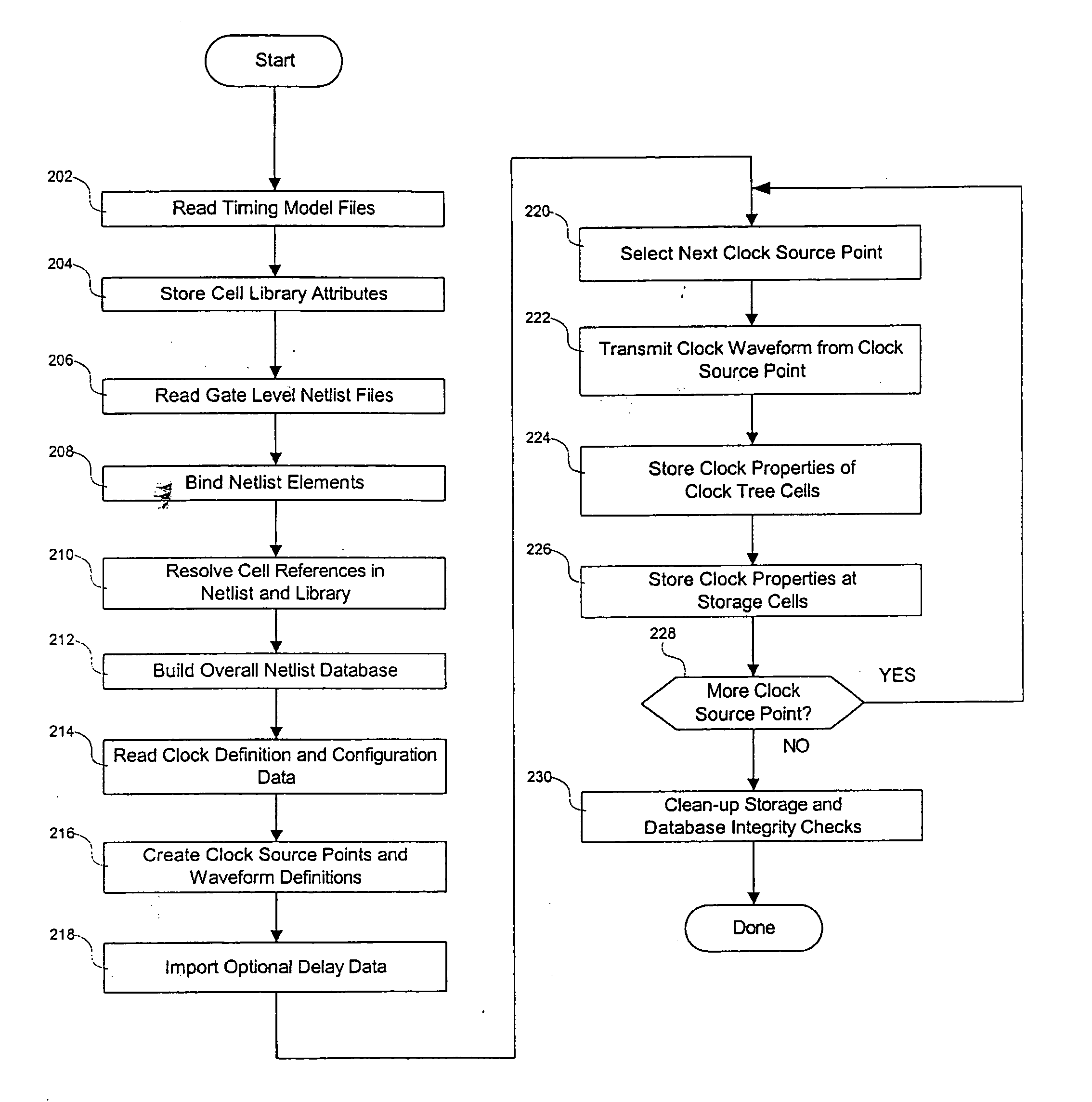
[0044] Various aspects will now be described in connection with exemplary embodiments including certain aspects described in terms of sequences of actions that can be performed by elements of a computer system. For example, it will be recognized that in each of the embodiments, the various actions can be performed by specialized circuits or circuitry (e.g., discrete and / or integrated logic gates interconnected to perform a specialized function), by program instructions being executed by one or more processors, or by a combination of both. Thus, the various aspects can be embodied in many different forms, and all such forms are contemplated to be within the scope of what is described. The instructions of a computer program for providing a design profile validation as illustrated in FIG. 6 can be embodied in any computer readable medium for use by or in connection with an instruction execution system, apparatus, or device, such as a computer based system, processor containing system, ...


PUM


Abstract

A method for analyzing and validating clock integration properties in a circuit design is disclosed. A database of timing points that are clocked cell elements of the circuit design is generated. Next, a timing point frame showing the interaction of the clocked cell elements and the non-clocked cell elements is generated. The timing point frame graphically shows the timing network properties for the cell elements of the circuit design. A clock analysis view can be generated from the timing point frame for selected timing points. In this respect, the timing point frame shows timing points that meet a prescribed criteria (e.g., same clock domain). Therefore, the clock analysis view provides a graphical representation of timing and clock interactions for the circuit design.

Description

FIELD OF THE INVENTION [0001] The present invention generally relates to timing and functional analysis in circuit designs and more specifically to a method for visually representing timing and clock relationships between circuit elements of an integrated circuit whereby graphical views of clock interactions are presented to a designer for further evaluation. BACKGROUND OF THE INVENTION [0002] The development of Very Large Scale Integrated (VLSI) chips can be divided into two broad design phases: logical (or front end) and physical (or back end). The logical design phase deals primarily with the functional aspects of the VLSI chip, while the physical design phase focuses on implementing the chip. A chip designer in the logical design phase typically starts with a high level specification and refines it through a number of levels of abstraction. The chip is then implemented in the physical design phase. The designer is careful to maintain functional equivalence between successive lev...

Claims


Application Information

Patent Timeline
Patent Type & Authority Applications(United States)
IPC IPC(8): G06F17/50
CPCG06F17/5022G06F2217/84G06F2217/62G06F17/509G06F30/18G06F30/396G06F30/33G06F2119/12G06F30/3315G06F2117/04
Inventor KUANG, SER-HOUMURPHY, SEAN KEVIN
Owner PICOCRAFT DESIGN SYST
Why Eureka
Try Eureka