

Sonic energy process chamber
a process chamber and sonic energy technology, applied in the direction of volume metering, optical radiation measurement, instruments, etc., can solve the problems of increasing manufacturing costs, existing machines, and relatively large consumption of process chemicals and water
- Summary
- Abstract
- Description
- Claims
- Application Information
AI Technical Summary
Benefits of technology
Problems solved by technology
Method used
Image

Examples
Embodiment Construction
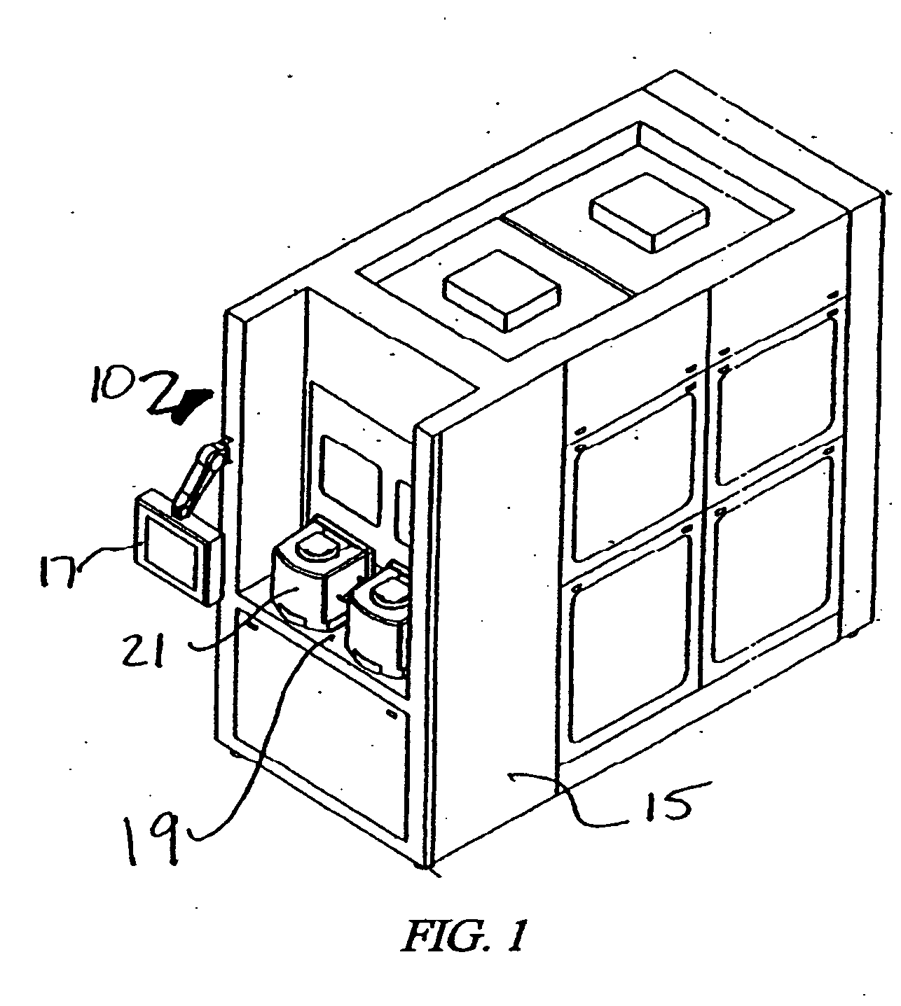
[0031] As shown in FIG. 1, a processing system 10 has an enclosure 15, a control / display 17, and an input / output station 19. Wafers or workpieces 24 within pods or boxes 21 (e.g., FOUPs) are removed from the boxes 21 at the input / output station 19 and processed within the system 10.
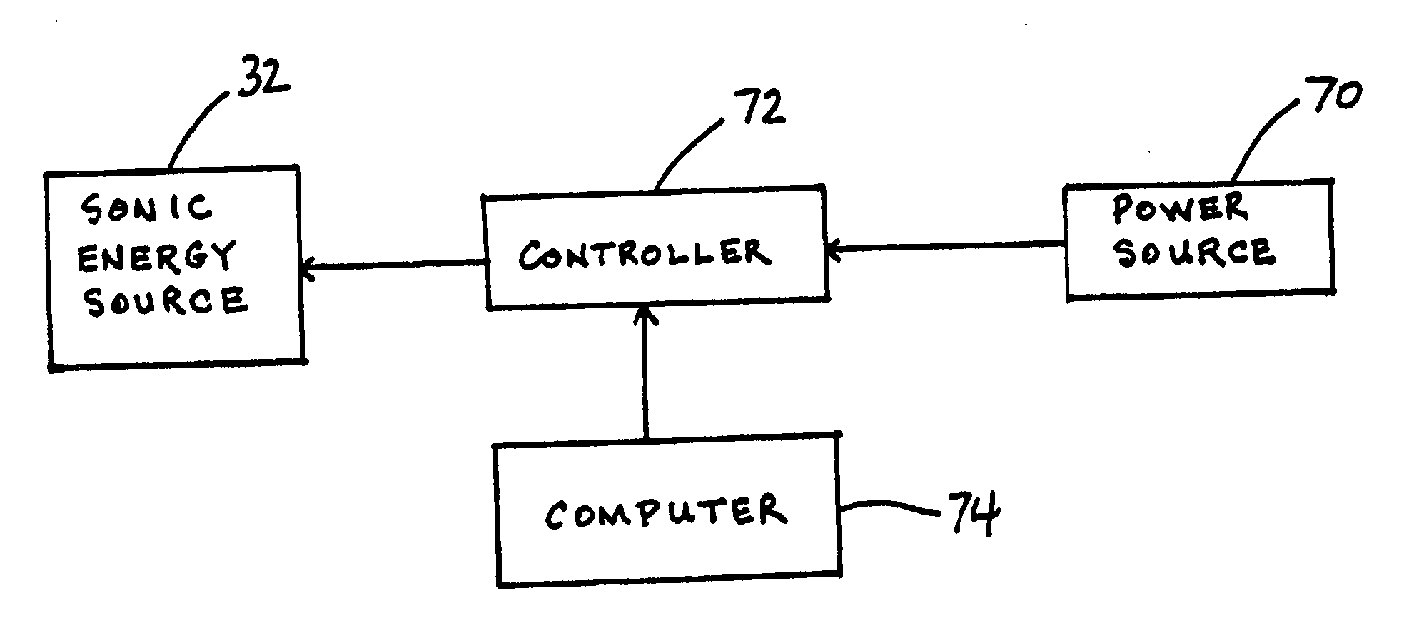
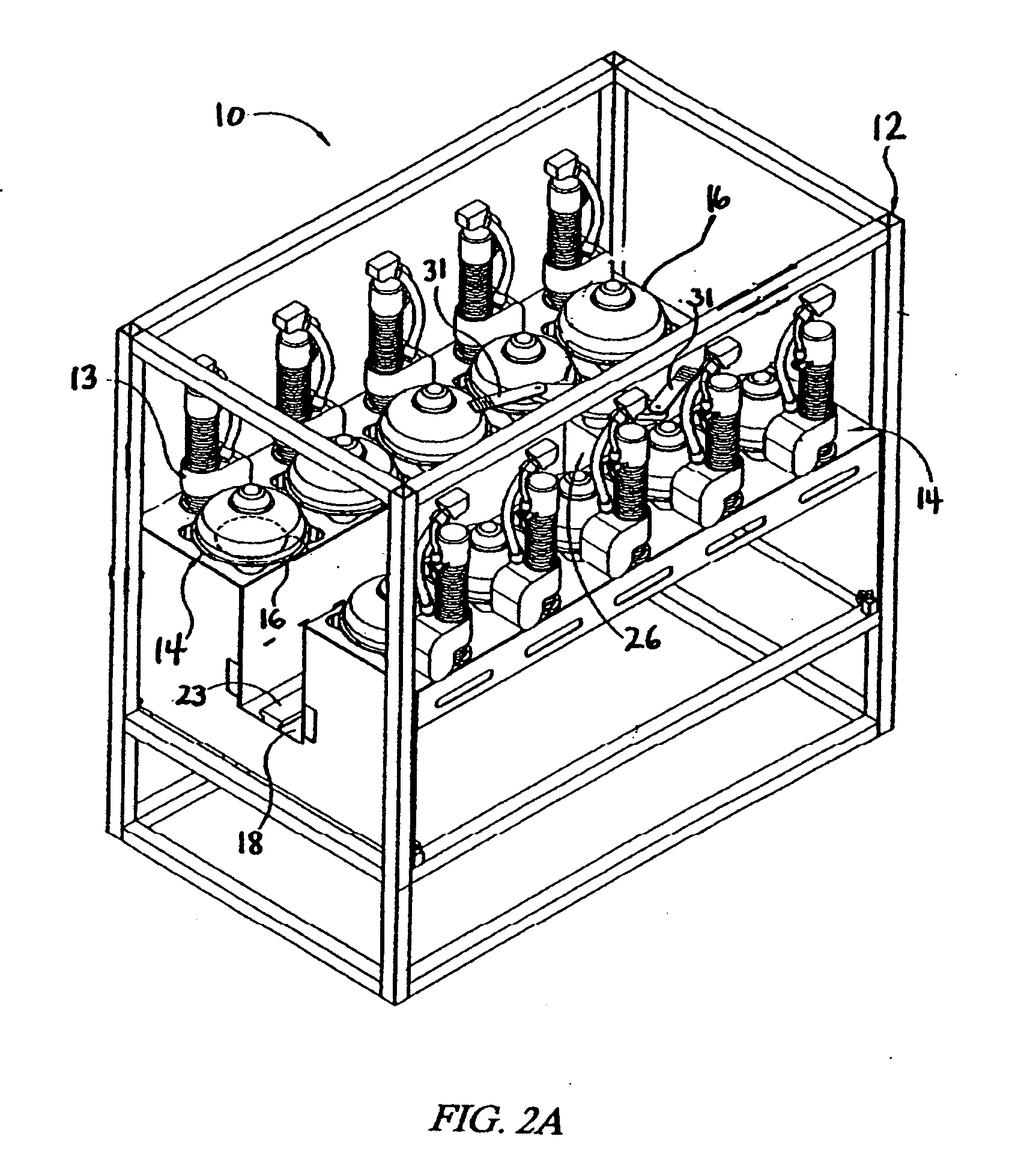
[0032] Turning to FIGS. 2A and 2B, the processing system 10 includes a support structure frame 12 with a plurality of processing stations 14 within the enclosure 15. A processing station 14 includes a process chamber 16 and a lift / rotate actuator 13. The process chamber 16 may be configured to process workpieces 24, such as 200 or 300 mm diameter semiconductor wafers provided within sealed boxes 21, open cassettes, or other carrier or container. The workpiece process chamber 16 of the present invention is designed to be utilized in a processing system 10, for example, as disclosed in pending U.S. patent application Ser. Nos. 10 / 733,807 filed Dec. 11, 2003, Ser. No. 10 / 859,748 filed Jun. 3, 2004, Ser. No....
PUM
| Property | Measurement | Unit |
|---|---|---|
| Fraction | aaaaa | aaaaa |
| Fraction | aaaaa | aaaaa |
| Fraction | aaaaa | aaaaa |
Abstract
Description
Claims
Application Information