High power LED package

Inactive Publication Date: 2005-09-15
SAMSUNG ELECTRO MECHANICS CO LTD
View PDF9 Cites 54 Cited by
  • Summary
  • Abstract
  • Description
  • Claims
  • Application Information

AI Technical Summary

Benefits of technology

[0013] The present invention has been made to solve the foregoing problems of the prior art and it is therefore an object of the present inv

Problems solved by technology

However, the LEDs also fail to covert electricity into light for 100%, thereby creating a considerable amount of heat.
As a consequence, the LEDs adopt metal lead frames to radiate heat to the outside because internal components of the LEDs become stressed owing to their thermal expansion coefficient difference if heat is not properly radiated.
However

Method used


Image

  • High power LED package
  • High power LED package
  • High power LED package

Examples


first embodiment

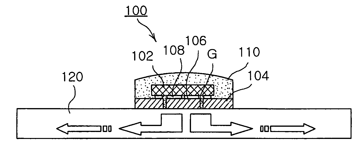
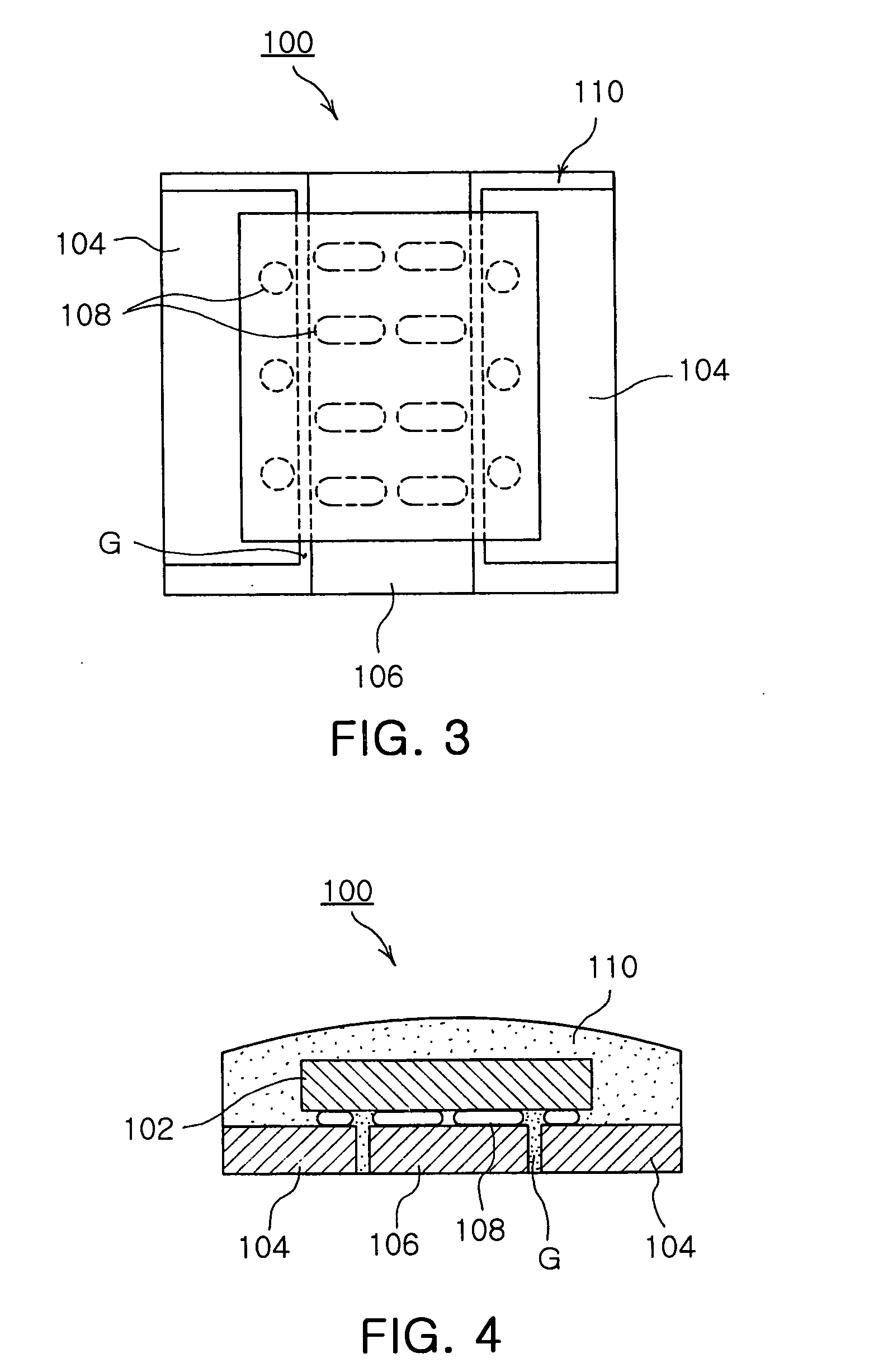
[0039]FIG. 3 is a plan view illustrating a high power LED package according to the invention, and FIG. 4 is a sectional view illustrating the high power LED package in FIG. 3.

[0040] Referring to FIGS. 3 and 4, a high power LED package 100 according to the first embodiment of the invention includes a LED chip 102 seated on substantially planar first and second lead frames 104 and 106 spaced apart from each other for predetermined gaps G. A package body 110 made of resin fixedly secures the underlying lead frames 104 and 106 in the bottom thereof while sealing the LED chip 102 therein.

[0041] The first lead frames 104 are constituted of two parts that are placed adjacent to both sides of the second lead frame 106 and spaced from the same for the gap G. Both the first and second lead frames 104 and 106 are made of high reflectivity metal to effectively reflect light from the LED chip 102 in an upward direction. The first and second lead frames 104 and 106 are preferably made of Ag or p...

sixth embodiment

[0064] Hereinafter an LED package fabrication method of the invention for obtaining LED packages 600 of the sixth embodiment as shown in FIGS. 14 and 15 will be described with reference to FIGS. 17 to 20.

[0065] First, a number of LED chips 602 are prepared, and solder bumps 608 are attached on electrodes as shown in FIG. 17.

[0066] The LED chips 602 with the solder bumps 608 are turned upside down and seated on seating sections 604a and 606a of a lead frame sheet 604, 606, in which a number of first and second lead frames are connected in succession as shown in FIG. 18.

[0067] Next encapsulant resin such as silicone is dispensed onto the LED chips 602 and the seating sections 604a and 606a to form encapsulants 610 as shown in FIG. 19. Optionally, transfer molding may be carried out with a mold so that the encapsulants 610 have a uniform convex geometry.

[0068] In FIG. 20, a desired resin is applied on the entire structure including the encapsulants 610 and the lead frame sheet 604, ...


PUM


Abstract

A high power LED package, in which substantially planar first and second lead frames made of high reflectivity metal are spaced from each other for a predetermined gap. An LED chip is seated on at least one of the lead frames, and having terminals electrically connected to the lead frames, respectively. A package body made of resin seals the LED chip therein while fixedly securing the lead frame in the bottom thereof. The encapsulant preferably fills up the gap between the first and second lead frames. The LED package is structured to raise thermal radiation efficiency thereby reducing the size and thickness thereof.

Description

CLAIM OF PRIORITY [0001] This application claims the benefit of Korean Patent Application No. 2004-17442 filed on Mar. 15, 2004, in the Korean Intellectual Property Office, the disclosure of which is incorporated herein by reference. BACKGROUND OF THE INVENTION [0002] 1. Field of the Invention [0003] The present invention relates to a Light Emitting Diode (LED) package, and more particularly, a high power LED package structured to raise thermal radiation efficiency thereby reducing the size and thickness thereof. [0004] 2. Description of the Related Art [0005] LEDs are one type of semiconductors, and generate various colors of light when applied with voltage. The color of light generated from each LED is generally determined by chemical ingredients of the LED. The LEDs are continuously increasing in demand since they has various merits such as long lifetime, low drive voltage, excellent initial drive properties, high vibration resistance and high tolerance with respect to repeated p...

Claims


Application Information

Patent Timeline
IPC IPC(8): H01L27/15H01L33/48H01L33/54H01L33/60H01L33/62
CPCH01L33/486H01L33/54H01L33/60H01L33/62H01L24/73H01L2224/16245H01L2224/48247H01L24/17H01L24/97H01L2924/12041H01L2224/48091H01L2924/00014H01L2924/00B63H5/165B26D1/30B26D5/10B26D2001/006
Inventor LEE, SEON GOOPARK, SEUNG MOPARK, CHAN WANGPARK, JUNG KYU
Owner SAMSUNG ELECTRO MECHANICS CO LTD
Why Eureka
Try Eureka