

Semiconductor device and electronic device
a technology of semiconductor devices and electronic devices, applied in semiconductor devices, semiconductor/solid-state device details, electrical apparatus, etc., can solve the problems of generating noise, single use of the above-mentioned two-input system which inputs complementary signals cannot fundamentally solve the drawback, and achieves low noise amplifier and signal wave distortion, the effect of reducing cross talk between the signal lines
- Summary
- Abstract
- Description
- Claims
- Application Information
AI Technical Summary
Benefits of technology
Problems solved by technology
Method used
Image

Examples
embodiment 1
[0088]FIG. 1 to FIG. 13 are views related to a semiconductor device (high frequency power module) of one embodiment (embodiment 1) of the present invention and a radio communication device in which the high frequency power module is incorporated. FIG. 1 to FIG. 5 are views related with the high frequency power module, FIG. 6 to FIG. 11 are views related to a manufacturing method of the high frequency power module, and FIG. 12 and FIG. 13 are views related to a radio communication device.
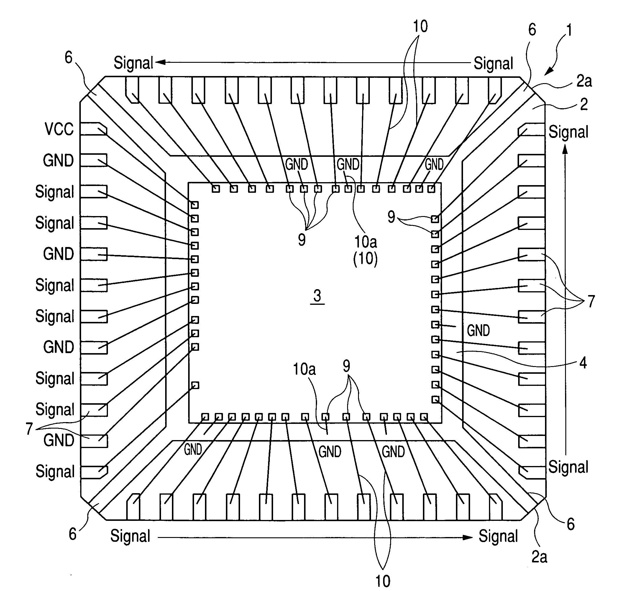
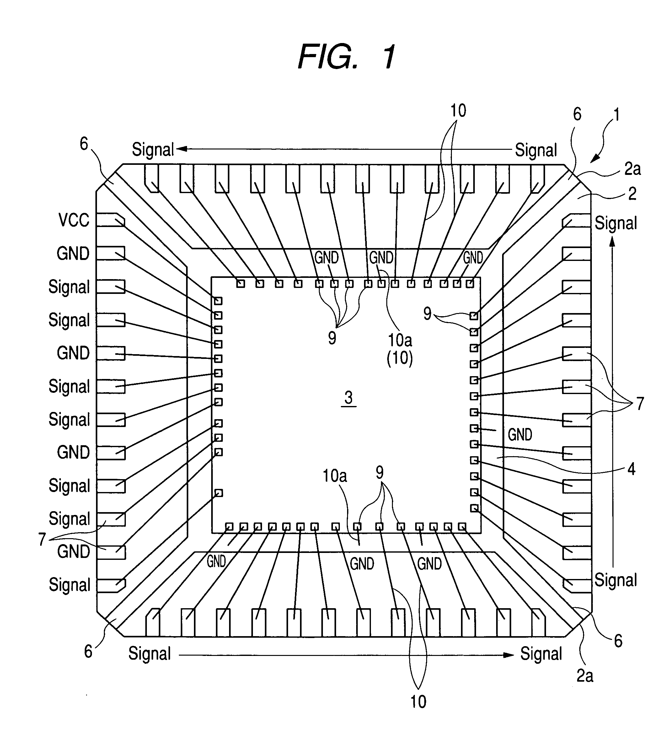
[0089] In this embodiment 1, the explanation is made with respect to an example in which the present invention is applied to a QFN type semiconductor device in which a tab, tab suspending leads contiguously formed with the tab and leads (external electrode terminals) are exposed on a mounting surface formed over a back surface of a quadrangular sealing body (package). The semiconductor device 1 forms the high frequency power module, for example.
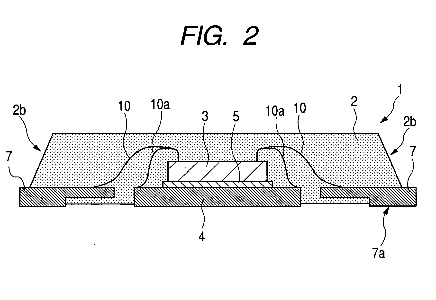
[0090] The QFN type semiconductor device 1, as shown i...
embodiment 2
[0154]FIG. 14 is a schematic plan view of a high frequency power module of another embodiment (embodiment 2) of the present invention in a state that a portion of a sealing body is cut away.
[0155] In the embodiment 1, the circuit parts include three low noise amplifiers (LNA) 24 as the specific circuit parts 11. In this embodiment 2, besides the above-mentioned circuit parts, among the VCO, the RFVCO 44 which treats the high frequency is also used as the specific circuit part 11. Accordingly, all the grounding electrode terminals 9 of the RFVCO 44 are connected to the leads (ground leads) 7 through the wires 10, while the ground electrode terminals 9 are not connected with the tab 4 through the wires.
[0156] With respect to the lines which reach the leads 7 from the electrode terminals 9 of the semiconductor chip 3 through the wires 10, the ground lines are arranged at both sides of two signal lines of the RFVCO 44 and hence, the electromagnetic shielding of the signal lines is pro...
embodiment 3
[0158]FIG. 15 is a schematic plan view of a high frequency power module of another embodiment (embodiment 3) of the present invention in a state that a portion of a sealing body is cut away.
[0159] This embodiment 3 is directed to an example in which the RFVCO 44 is provided as an exteriorly mounted part and hence, the semiconductor chip 3 is not formed in a monolithic manner. In this dual band communication method, the respective circuit parts such as the low noise amplifier, the mixer, the VCO, the synthesizer, the IQ modulator / demodulator, the frequency divider, the DC-AC modulator and the like are formed in a monolithic manner.
[0160] Two mixers in the reception system are respectively controlled by the frequency divider, and the frequency divider is a frequency converting circuit for converting the high frequency signal outputted from the RFVCO 44 which is the exteriorly mounted part into the low frequency signal.
[0161] Accordingly, in this embodiment 3, as shown in FIG. 15, t...
PUM
 Abstract
Description
Claims
Application Information