Semiconductor integrated circuit

a technology of integrated circuits and semiconductors, applied in the direction of vessel construction, pulse technique, separation process, etc., can solve the problems of small voltage drop occurring in a resistive component of the power line, affecting the delay of the signal, and increasing the load of the design work, so as to reduce the load of layout design, the degree of freedom of arrangement of the power switch cells, and the effect of suppressing the voltage drop of the power due to the power switch cells

Active Publication Date: 2005-09-15
SONY CORP
View PDF3 Cites 29 Cited by
  • Summary
  • Abstract
  • Description
  • Claims
  • Application Information

AI Technical Summary

Benefits of technology

[0023] According to one embodiment of the present invention, the degree of freedom of arrangement of the power switch cells becomes high, and automatic design of the layout by the CAD device can be easily realized, so the load of the layout design can be reduced.
[0024] Further, the voltage drop of the power due to the power switch cells can be suppressed, so the influence of the voltage drop occurring in the power switch cells exerted upon the signal delay can be reduced.

Problems solved by technology

For this reason, there are the disadvantages that the load of the design work increases, and the development period of the product becomes long.
Further, along with the reduction of the power supply voltage, a slight voltage drop occurring in a resistive component of the power line starts to exert a large influence upon the delay of the signal.
Namely, the lower the power supply voltage, the smaller the margin of the signal amplitude with respect to the threshold voltage of a transistor, so a large signal delay occurs even if the drop of the power supply voltage is small.
When a transistor switch is arranged in a power line under such a situation, the voltage drop due to this is further added, so the above problem becomes more serious.
Especially, the signal delay at the center of the circuit block where the distance from the external power line becomes long becomes large.
As a result, there is the problem that even if the circuit block normally operates by itself, it no longer operates when a transistor switch is arranged in the external power line.
Further, when the circuit block is further connected to a block of a higher level, there is the problem that the requested timing can no longer be satisfied.

Method used


Image

  • Semiconductor integrated circuit
  • Semiconductor integrated circuit
  • Semiconductor integrated circuit

Examples


first embodiment

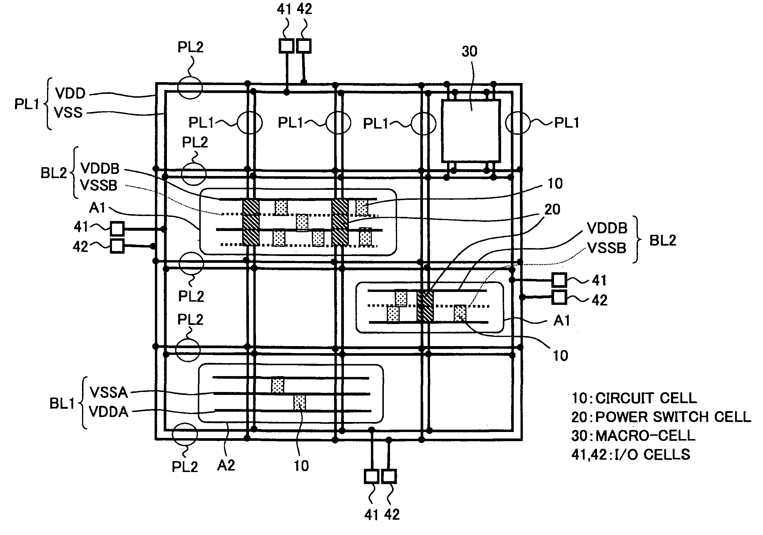
[0047]FIG. 1 is a view of an example of the configuration of a semiconductor integrated circuit according to a first embodiment of the present invention. In the figure, interconnect lines relating to the power and circuit cells connected to them are schematically illustrated.

[0048] The semiconductor integrated circuit shown in FIG. 1 has a plurality of groups of power lines PL1, a plurality of groups of power lines PL2, a plurality of groups of branch lines BL1 and BL2, a plurality of circuit cells 10, a plurality of power switch cells 20, a circuit block 30, and a plurality of power input cells 41 and 42.

[0049] Note that the groups of power lines PL1 are embodiments of the groups of power lines of the present invention, the groups of branch lines BL2 are embodiments of the groups of branch lines of the present invention, the circuit cells 10 are embodiments of the circuit cells of the present invention, and the power switch cells 20 are embodiments of the power switch cells of th...

second embodiment

[0070] Next, a second embodiment of the present invention will be explained.

[0071] The semiconductor integrated circuit according to the second embodiment shows the configurations of the power switch cells and circuit cells and the structures of the groups of branch lines connecting them in more detail than the semiconductor integrated circuit according to the first embodiment. The overall configuration such as the arrangement of the groups of power lines is the same as that of the semiconductor integrated circuit according to the first embodiment.

[0072]FIG. 4 is a view of an example of the configuration of a circuit cell 11 according to the second embodiment of the present invention. The circuit cell 11 shown in FIG. 4 has an inverter circuit configured as a serial circuit of a p-type MOS transistor Qp1 and an n-type MOS transistor Qn1 and has interconnect lines L111 and L112 supplying power to this inverter circuit. Note that while FIG. 4 shows an inverter circuit cell as one ex...

third embodiment

[0093] Next, a third embodiment of the present invention will be explained.

[0094] The semiconductor integrated circuit according to the third embodiment is obtained by changing parts of the configurations of the power switch cells and the interconnect line structures in the second embodiment explained above. The overall configuration such as the arrangement of the groups of power lines and the configuration of the circuit cells are the same as those of the semiconductor integrated circuits according to the first and second embodiments.

[0095]FIG. 7 is a view of an example of the configuration of a power switch cell 22 according to the third embodiment of the present invention. The power switch cell 22 has an n-type MOS transistor Qn3 and interconnect lines L221 to L223. The n-type MOS transistor Qn3 is an embodiment of the switch circuit of the present invention, the interconnect line L221 is an embodiment of the third interconnect line of the present invention, and the interconnec...


PUM

PropertyMeasurementUnit
poweraaaaaaaaaa
angleaaaaaaaaaa
areaaaaaaaaaaa

Abstract

A semiconductor integrated circuit able to reduce a load of layout design when arranging switches in a power lines for preventing leakage current and able to reduce the influence of a voltage drop occurring in the switches on a signal delay, wherein a plurality of groups of power lines are arranged in stripe shapes, power is supplied to circuit cells by a plurality of groups of branch lines branching from the groups of power lines, power switch cells arranged in the groups of branch lines turn on or off the supply of power to the circuit cells, the power switch cells are arranged dispersed in the area of arrangement of the circuit cells, and the supply of power by the power switch cells is finely controlled for every relatively small number of circuit cells.

Description

CROSS REFERENCES TO RELATED APPLICATION [0001] The present invention contains subject matter related to Japanese Patent Application JP 2004-067489 filed in the Japanese Patent Office on Mar. 10, 2004, the entire contents of which being incorporated herein by reference. BACKGROUND OF THE INVENTION [0002] 1. Field of the Invention [0003] The present invention relates to a semiconductor integrated circuit, more particularly relates to a semiconductor integrated circuit achieving a reduction of power consumption by using a transistor having a high threshold voltage to cut the supply of power to an unused circuit. [0004] 2. Backgound Art [0005] The power supply voltage of semiconductor integrated circuits have fallen year by year along with the reduction of the power consumption and the miniaturization of processing dimensions. When a signal amplitude becomes small due to the reduction of the power supply voltage, the threshold voltage of a transistor becomes high relative to the signal ...

Claims


Application Information

Patent Timeline
Patent Type & Authority Applications(United States)
IPC IPC(8): H01L23/522H01L23/528H01L21/822H01L27/00H01L27/02H01L27/04H03K19/177
CPCH01L23/5286H01L27/0203H01L27/11807H03K19/0013H01L2924/0002H03K19/0016H01L2924/00B63J2/12H05B3/02B01D35/02B01F23/40B01F27/80
Inventor OGATA, HIROMI
Owner SONY CORP
Why Eureka
Try Eureka