

Semiconductor output circuit
- Summary
- Abstract
- Description
- Claims
- Application Information
AI Technical Summary
Benefits of technology
Problems solved by technology
Method used
Image

Examples
first embodiment
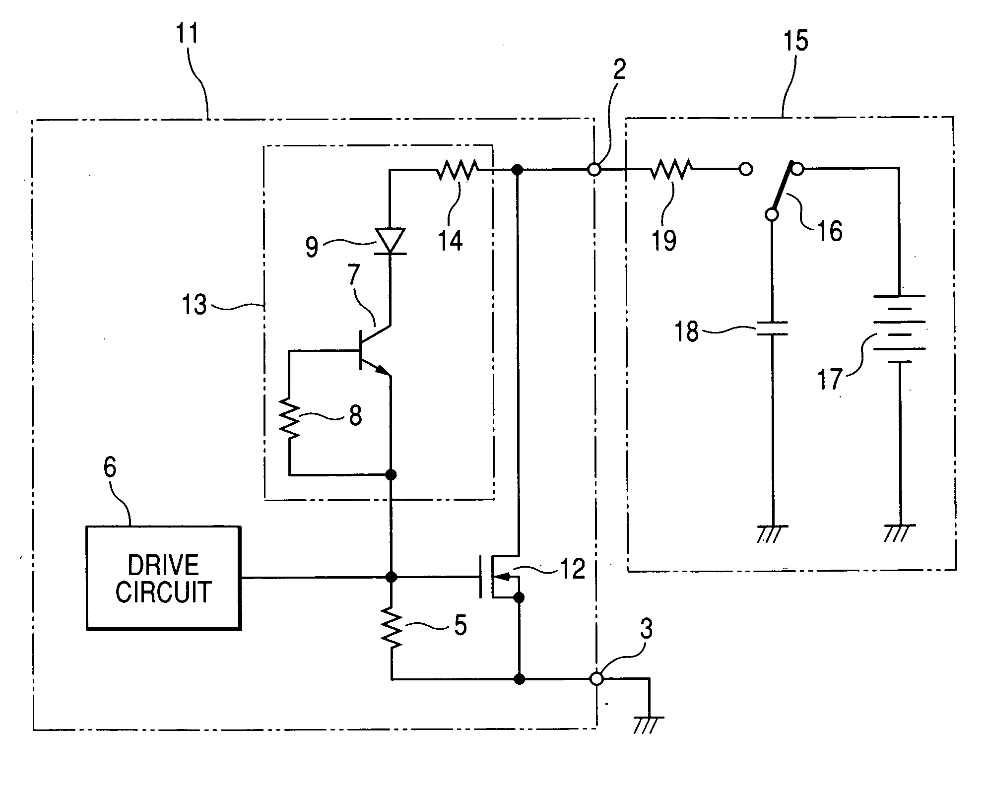
[0031]FIG. 1 shows a structure of a semiconductor output circuit 11 according to a first embodiment of the invention, and a structure of an ESD test device 15 used for testing the resistance to ESD of the semiconductor output circuit 11. For example, the semiconductor output circuit 11 can be used for an electronic control unit implemented as an IC or an intelligent IC to be mounted on a vehicle (automobile) that includes a CPU, a digital circuit, memories, an analog circuit, and a power supply circuit.
[0032] As shown in this figure, this semiconductor output circuit 11 includes an n-channel type LDMOS transistor 12, a drive circuit 6, a protective circuit 13, and external terminals 2, 3. The external terminals 2, 3 are connected to the drain and source of the MOS transistor 12, respectively. The gate and source of the MOS transistor 12 are electrically connected to each other by a resistor 5 for the purpose of pulling down the gate potential of the MOS transistor 12 to the ground ...
case b
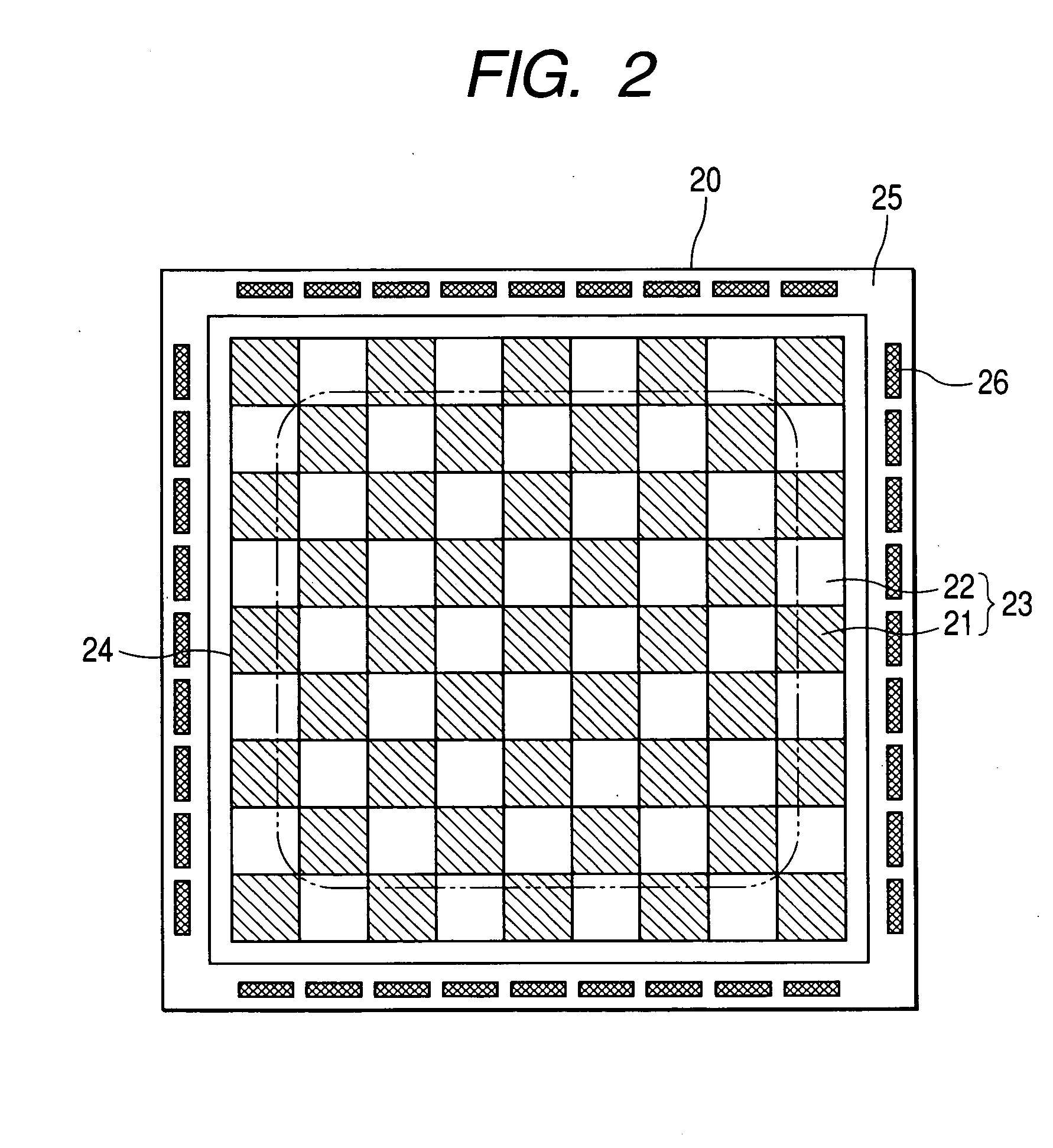
[0045] If a spike voltage is applied to the terminal 2 of the semiconductor output circuit 11 provided with the protective circuit 13, a surge current flows through the resistor 14, the diode 9, and the collector / base capacitance (junction capacitance) of the transistor 7. As a consequence, the gate voltage of the MOS transistor 12 increases. Accordingly, not only the unit transistors within the inner portion of the cell area 24 but also the unit transistors within the outer portion of the cell area 24 are turned on if the spike voltage is applied to the terminal 2, so that all the unit transistors in the cell area 24 can be prevented from entering the negative resistance region.
[0046] However, in a case where the protective circuit 13 does not have the resistor 14 as is the case with the prior art circuit shown in FIG. 11, if a spike voltage is applied to the terminal 2, the gate voltages of the unit transistors within the outer portion of the cell area 24 increase faster than tho...
second embodiment
[0060]FIG. 9 shows a structure of a semiconductor output circuit 27 according to a second embodiment of the invention. The second embodiment is different from the first embodiment in that, a protective circuit 28 includes the resistor 14 connected between the emitter of the transistor 7 and the node of the resistor 5, the gate of the MOS transistor 12 and the output of the driver circuit 6. Except for that, the semiconductor output circuit 27 according to the second embodiment operates in the same way as the semiconductor output circuit 11 according to the first embodiment.
PUM
 Abstract
Description
Claims
Application Information