Passivated nanoparticles, method of fabrication thereof, and devices incorporating nanoparticles

a technology of nanoparticles and passivating, which is applied in the field of passivating nanoparticles, can solve the problems of reducing the quantum efficiency of radiation and the production yield of nanoparticles, negatively affecting the optical and electrical properties of nanoparticles, and affecting the commercialization of nanoparticles

Inactive Publication Date: 2005-09-15
RENESSELAER POLYTECHNIC INST
View PDF12 Cites 39 Cited by
  • Summary
  • Abstract
  • Description
  • Claims
  • Application Information

AI Technical Summary

Problems solved by technology

However, this method is disadvantageous because it involves the use of a high temperature (above 200° C.) process and toxic reactants and surfactants.
The organic surfactant negatively affects the optical and electrical properties of the nanoparticles.
However, the shell also interferes with the optical and electrical properties of the nanoparticles, decreasing quantum efficiency of the radiation and the production yield of the nanoparticles.
The commercialization of the nanoparticles has also been hampered due to the high cost of production of the nanoparticles.
The methods used for synthesis are extremely toxic at high temperatures and hence pose significant safety problems during mass production.
Furthermore, it has been difficult to form nanoparticles of a uniform size.
However, the present inventor has determined that both of these methods do not lead to an accurate determination of nanoparticle size in the solution.
Using the absorption spectra exciton peak position to approximate nanoparticle size is problematic for a different reason.
However, when the present inventor arranged for the size of these EviDots® nanoparticles to be measured by a photon correlated spectroscopy (PCS) method, the results indicated that the nanoparticles in the solution have agglomerated into large clusters and have a non-uniform size distribution.
Thus, while the agglomerated nanoparticles have acceptable optical properties, they have unacceptable mechanical properties due to the agglomeration for uses which require a precise size distribution, such as for biological marker use.

Method used


Image

  • Passivated nanoparticles, method of fabrication thereof, and devices incorporating nanoparticles
  • Passivated nanoparticles, method of fabrication thereof, and devices incorporating nanoparticles
  • Passivated nanoparticles, method of fabrication thereof, and devices incorporating nanoparticles

Examples


example 1

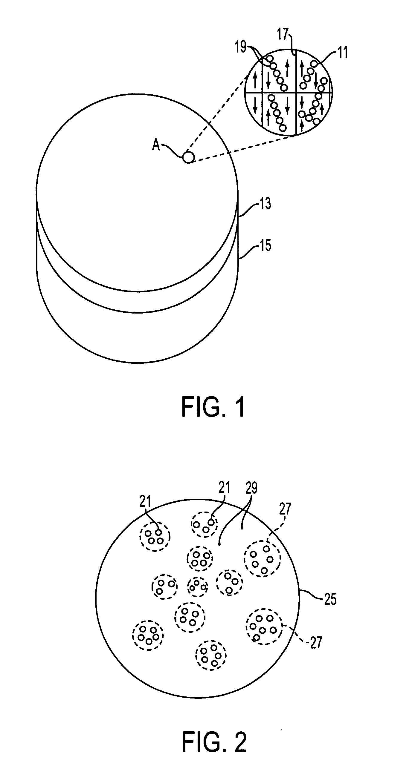
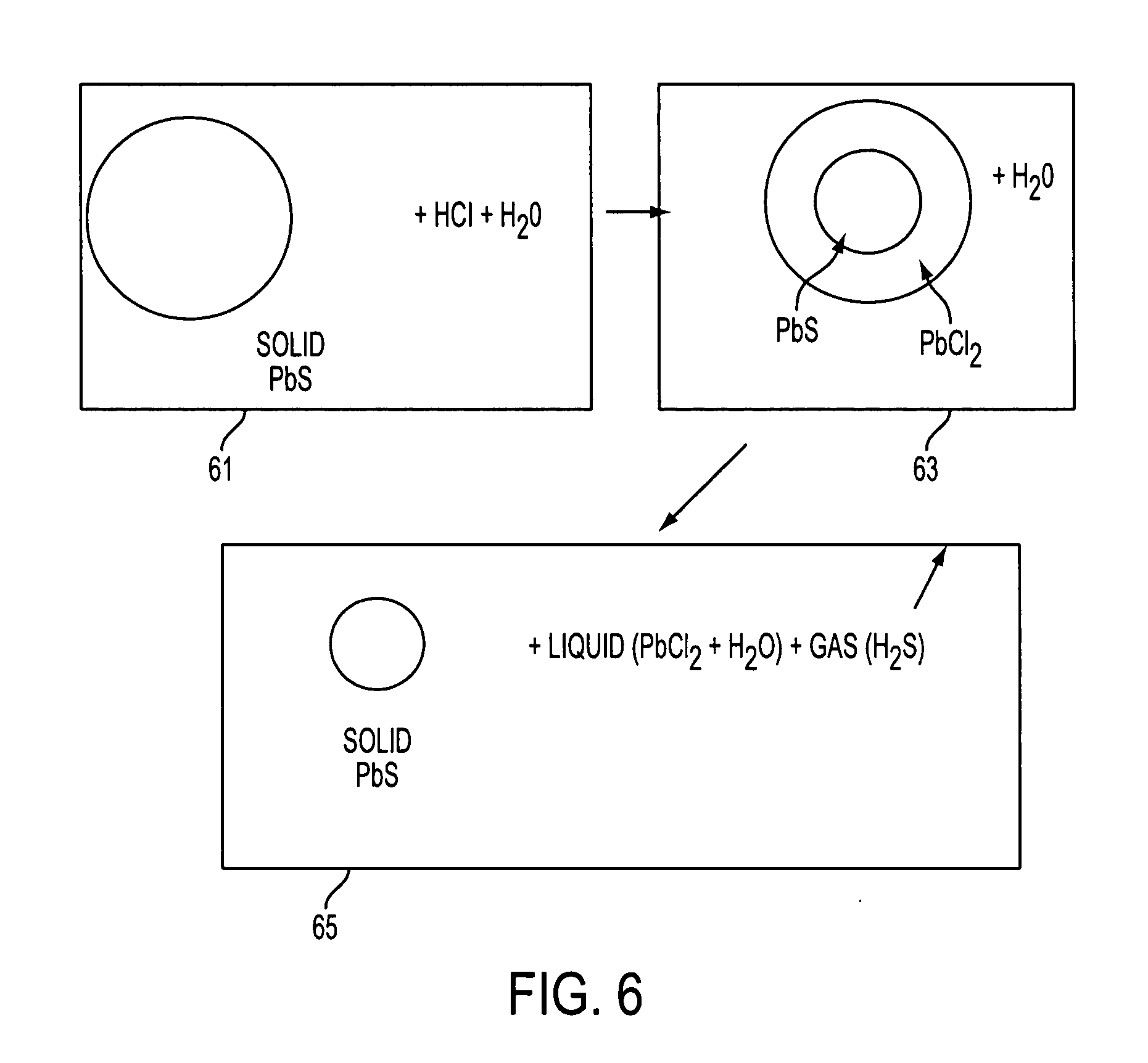
[0091] PbS nanoparticles according to the preferred embodiments of the present invention were prepared by the following method. 2 grams of PbCl2 powder were dissolved in 100 ml of warm water at 60-70° C. 2 grams of Na2S powder were separately dissolved in 100 ml of warm water (60-70° C.). Both solutions were filtered using 20 nm pore filter paper. 5 ml of the above PbCl2 solution was added to 15 ml of above Na2S solution and mixed in an ultrasonic vibrator.

[0092] The nanoparticle containing solution was analyzed by photon correlated spectroscopy (PCS) using the N4 Plus Submicron Particle Analyzer made by Beckman Coulter, Inc. PCS is a dynamic light scattering (DLS) optical characterization technique which determines particle size based on Brownian motion of particles in a solution. In PCS, measurements of particle size are based on characterization of the time scale of fluctuations of the intensity of laser light scattered from the nanoparticle containing solution. The fluctuations...

example 2

[0094] In this example, the nanoparticles of example 1 were etched with diluted HCl. 1 ml of HCl was dissolved in 50 ml of H2O. 2 ml of the above solution was added to the nanoparticle containing solution of example 1. The PCS spectra of the solution containing the etched nanoparticles is shown in FIG. 8. The nanoparticles had a 53.3 nm average size with a standard deviation of 20.8 nm. Thus, adding HCl to the solution reduced the nanoparticle size without completely dissolving the nanoparticles.

example 3

[0095] In this example, the nanoparticles of example 2 were etched with additional diluted HCl. 1 ml of HCl was dissolved in 50 ml of H2O. 2 ml of the above solution was added to the nanoparticle containing solution of example 2. The PCS spectra of the solution containing the etched nanoparticles is shown in FIG. 9. The nanoparticles had a 17.6 nm average size with a standard deviation of 9.1 nm.


PUM

PropertyMeasurementUnit
sizeaaaaaaaaaa
sizeaaaaaaaaaa
temperatureaaaaaaaaaa

Abstract

A plurality of semiconductor nanoparticles having an elementally passivated surface are provided. These nanoparticles are capable of being suspended in water without substantial agglomeration and substantial precipitation on container surfaces for at least 30 days. The method of making the semiconductor nanoparticles includes reacting at least a first reactant and a second reactant in a solution to form the semiconductor nanoparticles in the solution. A first reactant provides a passivating element which binds to dangling bonds on a surface of the nanoparticles to passivate the surface of the nanoparticles. The nanoparticle size can be tuned by etching the nanoparticles located in the solution to a desired size.

Description

[0001] This application claims benefit of priority of U.S. provisional application Ser. No. 60 / 316,979, filed on Sep. 5, 2001, incorporated herein by reference in its entirety.FIELD OF THE INVENTION [0002] The present invention is directed generally to semiconductor materials and more particularly to passivated nanoparticles. BACKGROUND OF THE INVENTION [0003] Numerous patents and publication have been issued on the fabrication of semiconductor nanoparticles (also called “quantum dots” or “nanocrystals”) and their applications in the last few years. These semiconductor nanoparticles are used as a lasing medium in a laser, as fluorescent tags in biological testing methods and as electronic devices. [0004] A relatively new correlative method for easier manipulation and spatial organization of the nanoparticles has been proposed in which the nanoparticles are encapsulated in a shell. The shells which encapsulate the nanoparticles are composed of various organic materials such as Polyvi...

Claims


Application Information

Patent Timeline
Patent Type & Authority Applications(United States)
IPC IPC(8): C01G21/21C30B7/00C30B7/14
CPCB82Y30/00Y10T428/2991C01G21/21C01P2004/52C01P2004/64C01P2006/40C09D5/028C09D5/24C09D11/52C09K11/025C30B7/00C30B7/14C30B29/40C30B29/48C30B29/605H01L21/02521H01L21/02568H01L21/02601H01L21/02628H01L21/02664H01L51/5012Y10S977/888Y10S977/847Y10S977/778Y10S977/835Y10S977/856Y10S977/786Y10S977/813C01B19/007H10K50/11
Inventor DUTTA, PARTHA
Owner RENESSELAER POLYTECHNIC INST
Why Eureka
Try Eureka