Method of laser irradiation

a laser irradiation and laser beam technology, applied in the field of laser irradiation, can solve the problems of low electric field mobility (fe), insufficient capability to implement a liquid crystal display having a high, and excellent functions

Inactive Publication Date: 2005-09-15
KK TOSHIBA
View PDF2 Cites 16 Cited by
  • Summary
  • Abstract
  • Description
  • Claims
  • Application Information

AI Technical Summary

Benefits of technology

[0015] With the method of laser irradiation according to the present invention, the angle of the mirror is adjusted so that the short axis homogenizer can adjust the short axis-wise width of each laser beam. Then, the amorphous silicon semiconductor on the translucent substrate is irradiated with the laser beams each having its short axis-wise width adjusted. The intensity of each laser beam can be adjusted simply by adjusting the angle of the mirror. This makes it possible to properly adjust the intensity of the laser beam all over the surface of the translucent substrate.

Problems solved by technology

However, a thin film transistor using amorphous silicon, which has a low electric field mobility (μFE) of at most 1 cm2 / Vs, has capabilities insufficient to implement a liquid crystal display having a high definition, operating at high speed, and providing excellent functions.
Such microcrystal polysilicon does not provide desired transistor characteristics.
This disadvantageously affects the mass production of thin film transistors made of polysilicon.
About 20 times of pulse irradiations barely provide a fluence margin sufficient for production.
Thus, it is disadvantageously difficult to adjust the intensity of the laser beams.

Method used


Image

  • Method of laser irradiation
  • Method of laser irradiation
  • Method of laser irradiation

Examples


Embodiment Construction

[0021] With reference to the drawings, description will be given of a method of laser irradiation according to an embodiment of the present invention.

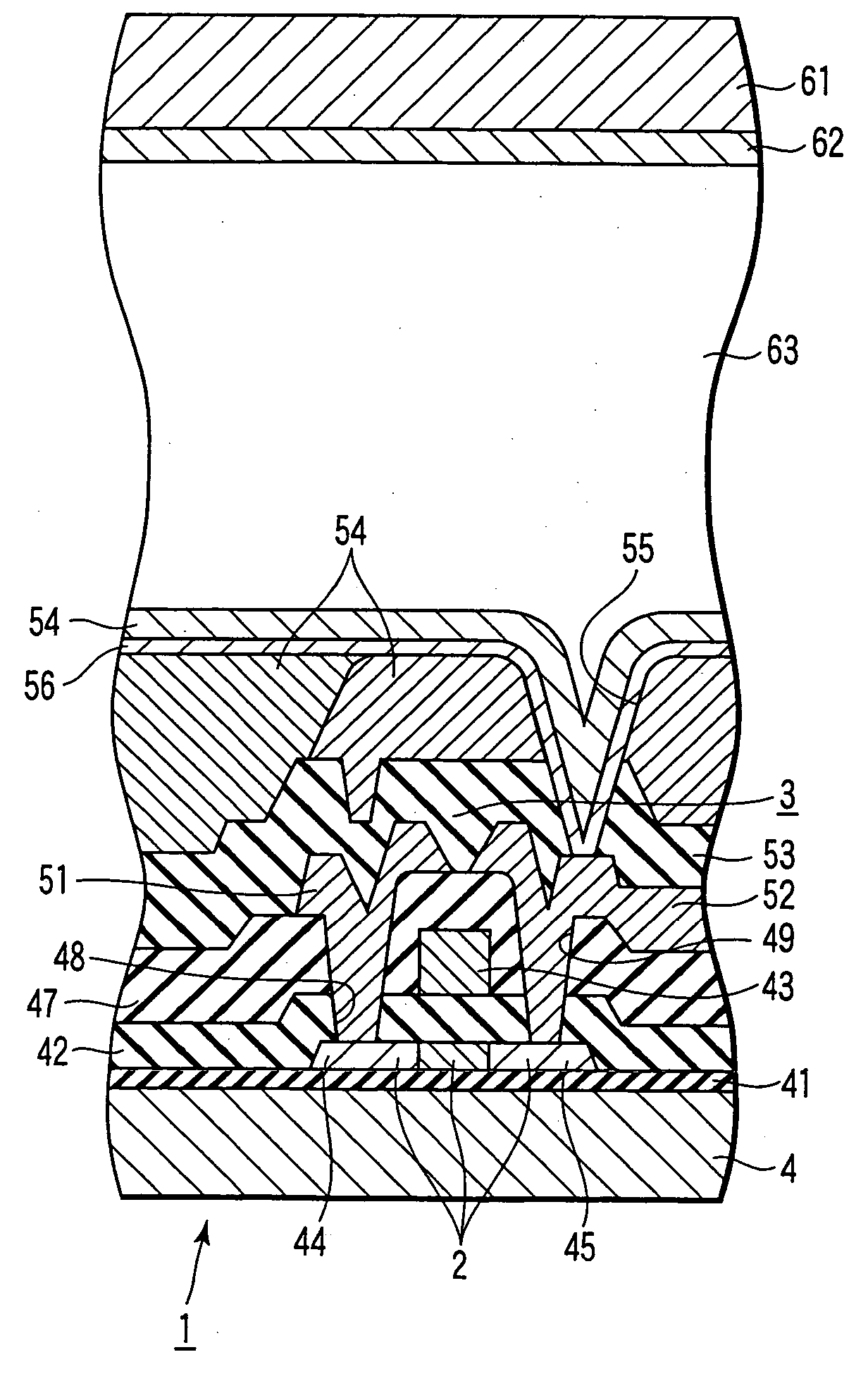
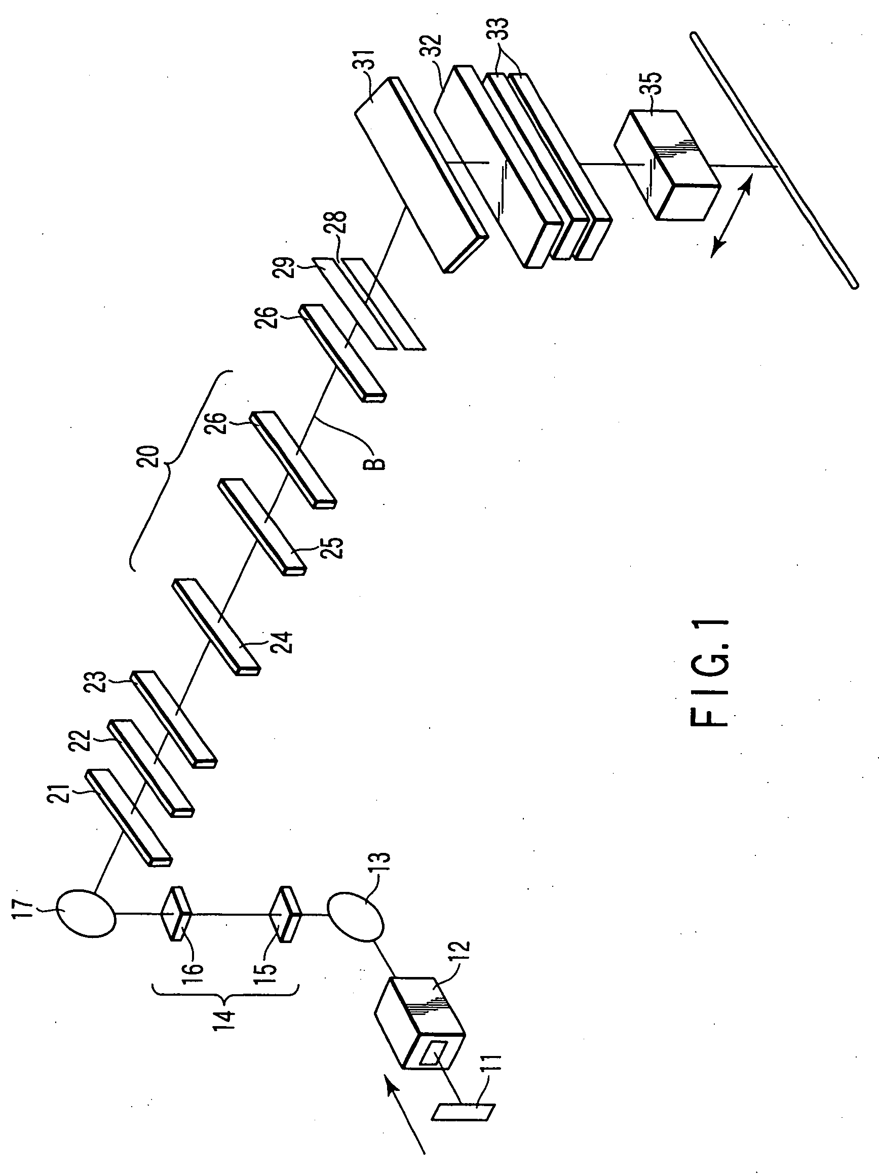
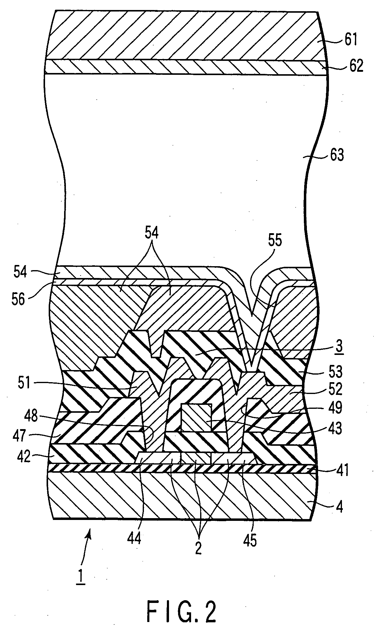
[0022] A laser anneal apparatus as a laser irradiation apparatus, shown in FIG. 1, is a part of an apparatus that manufactures a liquid crystal display (LCD) based on an active matrix system, shown in FIG. 2. The liquid crystal display shown in FIG. 2 comprises a insulated gate type thin film transistor (TFT) 3. The thin film transistor 3 is used as a pixel switch for the liquid crystal display and is formed by a polysilicon layer 2 on an array substrate 1.

[0023] The laser anneal apparatus shown in FIG. 1 irradiates a thin film of amorphous silicon with generally rectangular excimer laser beams B as linear beams emitted by a pulse laser such as xenon chloride (XeCl) laser, the thin film being formed on one major surface of a glass substrate 4 as a translucent substrate, shown in FIG. 2.

[0024] Then, the amorphous silicon layer locate...


PUM

PropertyMeasurementUnit
diameteraaaaaaaaaa
sizeaaaaaaaaaa
thicknessaaaaaaaaaa

Abstract

A method of laser irradiation including reflecting a linear laser beam from a mirror to bend an optical path of the laser beam, adjusting a width of the laser beam in the short axis direction of the laser beam whose optical path is bent by the mirror, by a short axis homogenizer, and irradiating an amorphous silicon semiconductor on a translucent substrate with the laser beam whose width in the short axis direction is adjusted by the short axis homogenizer, wherein the intensity of the laser beam is adjusted by adjusting the angle of the mirror.

Description

CROSS REFERENCE TO RELATED APPLICATIONS [0001] This is a Continuation Application of PCT Application No. PCT / JP03 / 10223, filed Aug. 11, 2003, which was published under PCT Article 21(2) in Japanese. [0002] This application is based upon and claims the benefit of priority from prior Japanese Patent Application No. 2002-236054, filed Aug. 13, 2002, the entire contents of which are incorporated herein by reference.BACKGROUND OF THE INVENTION [0003] 1. Field of the Invention [0004] The present invention relates to a method of laser irradiation with which an amorphous silicon film on a translucent substrate is irradiated with laser beams. [0005] 2. Description of the Related Art [0006] Liquid crystal displays (LCD) are now used which use, as a pixel switch, an insulated gate type thin film transistor (TFT) formed of amorphous silicon (a-Si). However, a thin film transistor using amorphous silicon, which has a low electric field mobility (μFE) of at most 1 cm2 / Vs, has capabilities insuffi...

Claims


Application Information

Patent Timeline
Patent Type & Authority Applications(United States)
IPC IPC(8): B23K26/06B23K26/067B23K26/073H01L21/20H01L21/428
CPCB23K26/0604B23K26/0608H01L21/2026B23K26/0738B23K26/067H01L21/02422H01L21/02532H01L21/02678H01L21/02686H01L21/26
Inventor MITSUHASHI, HIROSHIMIZOUCHI, KIYOTSUGUAWANO, TAKASHI
Owner KK TOSHIBA
Why Eureka
Try Eureka